Electrical characteristics, Absolute maximum ratings, Dc characteristics – Rainbow Electronics ATmega3290P_V User Manual
Page 313: Absolute maximum ratings* dc characteristics
313
ATmega329/3290/649/6490
2552H–AVR–11/06
Electrical Characteristics
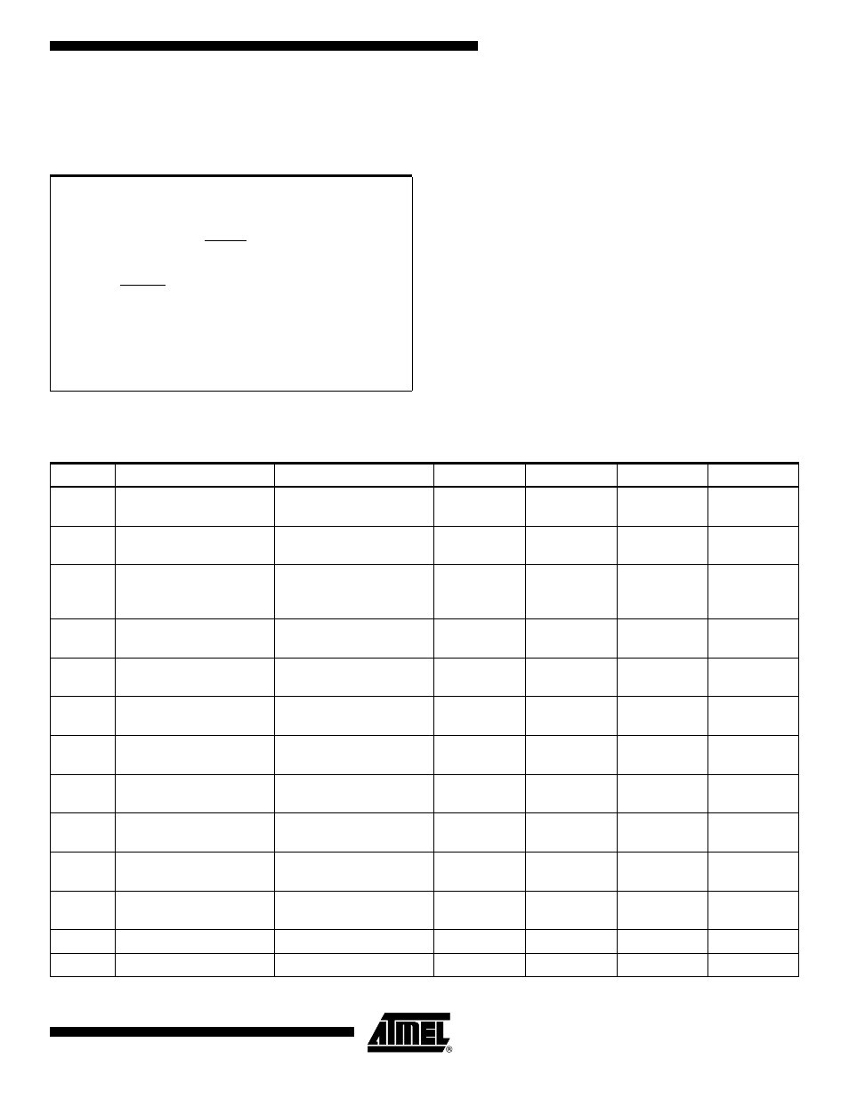
Absolute Maximum Ratings*
DC Characteristics
Operating Temperature.................................. -55
°C to +125°C
*NOTICE:
Stresses beyond those listed under “Absolute
Maximum Ratings” may cause permanent dam-
age to the device. This is a stress rating only and
functional operation of the device at these or
other conditions beyond those indicated in the
operational sections of this specification is not
implied. Exposure to absolute maximum rating
conditions for extended periods may affect
device reliability.
Storage Temperature ..................................... -65°C to +150°C
Voltage on any Pin except RESET
with respect to Ground ................................-0.5V to V
CC
+0.5V
Voltage on RESET with respect to Ground......-0.5V to +13.0V
Maximum Operating Voltage ............................................ 6.0V
DC Current per I/O Pin ............................................... 40.0 mA
DC Current
V
CC
and GND Pins................................ 200.0 mA
T
A
= -40
°C to 85°C, V
CC
= 1.8V to 5.5V (unless otherwise noted)
Symbol
Parameter
Condition
Min.
Typ.
Max.
Units
V
IL
Input Low Voltage, Except
XTAL1 pin
V
CC
= 1.8V - 2.4V
V
CC
= 2.4V - 5.5V
-0.5
-0.5
0.2V
CC
(1)
0.3V
CC
(1)
V
V
IL1
Input Low Voltage, XTAL1
pin
V
CC
= 1.8V - 5.5V
-0.5
0.1V
CC
(1)
V
V
IH
Input High Voltage,
Except XTAL1 and
RESET pins
V
CC
= 1.8V - 2.4V
V
CC
= 2.4V - 5.5V
0.7V
CC
(2)
0.6V
CC
(2)
V
CC
+ 0.5
V
CC
+ 0.5
V
V
IH1
Input High Voltage,
XTAL1 pin
V
CC
= 1.8V - 2.4V
V
CC
= 2.4V - 5.5V
0.8V
CC
(2)
0.7V
CC
(2)
V
CC
+ 0.5
V
CC
+ 0.5
V
V
IH2
Input High Voltage,
RESET pin
V
CC
= 1.8V - 5.5V
0.85V
CC
(2)
V
CC
+ 0.5
V
V
OL
Output Low Voltage
(3)
,
Port A, C, D, E, F, G, H, J
I
OL
= 10mA, V
CC
= 5V
I
OL
= 5mA, V
CC
= 3V
0.7
0.5
V
V
OL1
Output Low Voltage
(3)
,
Port B
I
OL
= 20mA, V
CC
= 5V
I
OL
= 10mA, V
CC
= 3V
0.7
0.5
V
V
OH
Output High Voltage
(4)
,
Port A, C, D, E, F, G, H, J
I
OH
= -10mA, V
CC
= 5V
I
OH
= -5mA, V
CC
= 3V
4.2
2.3
V
V
OH1
Output High Voltage
(4)
,
Port B
I
OH
= -20mA, V
CC
= 5V
I
OH
= -10mA, V
CC
= 3V
4.2
2.3
V
I
IL
Input Leakage
Current I/O Pin
V
CC
= 5.5V, pin low
(absolute value)
1
µA
I
IH
Input Leakage
Current I/O Pin
V
CC
= 5.5V, pin high
(absolute value)
1
µA
R
RST
Reset Pull-up Resistor
20
100
k
Ω
R
PU
I/O Pin Pull-up Resistor
20
100
k
Ω