Lcdccr - lcd contrast control register – Rainbow Electronics ATmega3290P_V User Manual
Page 234
234
ATmega329/3290/649/6490
2552H–AVR–11/06
LCDCCR – LCD Contrast
Control Register
• Bits 7:5 – LCDDC2:0: LDC Display Configuration
The LCDDC2:0 bits determine the amount of time the LCD drivers are turned on for
each voltage transition on segment and common pins. A short drive time will lead to
lower power consumption, but displays with high internal resistance may need longer
drive time to achieve satisfactory contrast. Note that the drive time will never be longer
than one half prescaled LCD clock period, even if the selected drive time is longer.
When using static duty or blanking, drive time will always be one half prescaled LCD
clock period.
New values take effect immediately, and can cause small glitches in the display output.
This can be avoided by setting the LCDBL in LCDCRA, and wait to the next start of
frame before changing LCDDC2:0.
Note:
The drive time will be longer dependent on oscillator startup time.
• Bit 4 – Res: Reserved Bit
This bit is reserved in the ATmega329/3290/649/6490 and will always read as zero.
• Bits 3:0 – LCDCC3:0: LCD Contrast Control
The LCDCC3:0 bits determine the maximum voltage V
LCD
on segment and common
pins. The different selections are shown in Table 106. New values take effect every
beginning of a new frame.
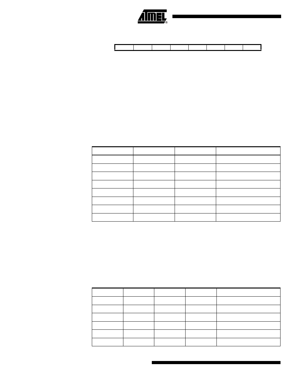
Bit
7
6
5
4
3
2
1
0
LCDDC2
LCDDC1
LCDDC0
–
LCDCC3
LCDCC2
LCDCC1
LCDCC0
LCDCCR
Read/Write
R/W
R/W
R/W
R
R/W
R/W
R/W
R/W
Initial Value
0
0
0
0
0
0
0
0
Table 105. LCD Display Configuration
LCDDC2
LCDDC1
LCDDC0
Nominal drive time
0
0
0
300 µs
0
0
1
70 µs
0
1
0
150 µs
0
1
1
450 µs
1
0
0
575 µs
1
0
1
850 µs
1
1
0
1150 µs
1
1
1
50% of clk
LCD_PS
Table 106. LCD Contrast Control
LCDCC3
LCDCC2
LCDCC1
LCDCC0
Maximum Voltage V
LCD
0
0
0
0
2.60
0
0
0
1
2.65
0
0
1
0
2.70
0
0
1
1
2.75
0
1
0
0
2.80
0
1
0
1
2.85