Analog comparator, Overview, Adcsrb - adc control and status register b – Rainbow Electronics ATmega3290P_V User Manual
Page 200
200
ATmega329/3290/649/6490
2552H–AVR–11/06
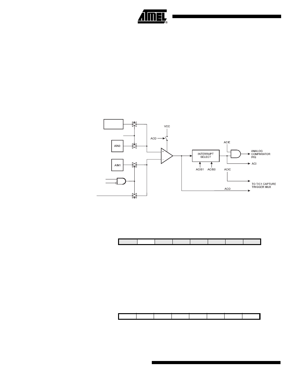
Analog Comparator
Overview
The Analog Comparator compares the input values on the positive pin AIN0 and nega-
tive pin AIN1. When the voltage on the positive pin AIN0 is higher than the voltage on
the negative pin AIN1, the Analog Comparator output, ACO, is set. The comparator’s
output can be set to trigger the Timer/Counter1 Input Capture function. In addition, the
comparator can trigger a separate interrupt, exclusive to the Analog Comparator. The
user can select Interrupt triggering on comparator output rise, fall or toggle. A block dia-
gram of the comparator and its surrounding logic is shown in Figure 83.
The PRADC, in “Power Reduction Register - PRR” on page 35 must be written to zero
to use the ADC input MUX.
Figure 83. Analog Comparator Block Diagram
(2)
Notes:
1. See Table 92 on page 202.
2. Refer to Figure 1 on page 2 and Table 29 on page 68 for Analog Comparator pin
placement.
ADCSRB – ADC Control and
Status Register B
• Bit 6 – ACME: Analog Comparator Multiplexer Enable
When this bit is written logic one and the ADC is switched off (ADEN in ADCSRA is
zero), the ADC multiplexer selects the negative input to the Analog Comparator. When
this bit is written logic zero, AIN1 is applied to the negative input of the Analog Compar-
ator. For a detailed description of this bit, see “Analog Comparator Multiplexed Input” on
page 202.
ACSR – Analog Comparator
Control and Status Register
ACBG
BANDGAP
REFERENCE
ADC MULTIPLEXER
OUTPUT
ACME
ADEN
(1)
Bit
7
6
5
4
3
2
1
0
–
ACME
–
–
–
ADTS2
ADTS1
ADTS0
ADCSRB
Read/Write
R
R/W
R
R
R
R/W
R/W
R/W
Initial Value
0
0
0
0
0
0
0
0
Bit
7
6
5
4
3
2
1
0
ACD
ACBG
ACO
ACI
ACIE
ACIC
ACIS1
ACIS0
ACSR
Read/Write
R/W
R/W
R
R/W
R/W
R/W
R/W
R/W
Initial Value
0
0
N/A
0
0
0
0
0