Rainbow Electronics ATmega3290P_V User Manual
Page 189
189
ATmega329/3290/649/6490
2552H–AVR–11/06
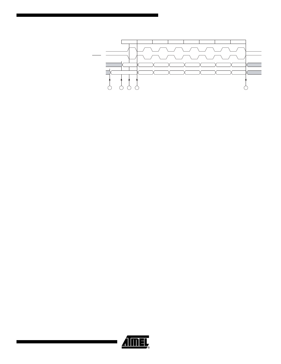
Figure 79. Three-wire Mode, Timing Diagram
The Three-wire mode timing is shown in Figure 79. At the top of the figure is a USCK
cycle reference. One bit is shifted into the USI Shift Register (USIDR) for each of these
cycles. The USCK timing is shown for both external clock modes. In External Clock
mode 0 (USICS0 = 0), DI is sampled at positive edges, and DO is changed (Data Regis-
ter is shifted by one) at negative edges. External Clock mode 1 (USICS0 = 1) uses the
opposite edges versus mode 0, i.e., samples data at negative and changes the output at
positive edges. The USI clock modes corresponds to the SPI data mode 0 and 1.
Referring to the timing diagram (Figure 79.), a bus transfer involves the following steps:
1.
The Slave device and Master device sets up its data output and, depending on
the protocol used, enables its output driver (mark A and B). The output is set up
by writing the data to be transmitted to the Serial Data Register. Enabling of the
output is done by setting the corresponding bit in the port Data Direction Regis-
ter. Note that point A and B does not have any specific order, but both must be at
least one half USCK cycle before point C where the data is sampled. This must
be done to ensure that the data setup requirement is satisfied. The 4-bit counter
is reset to zero.
2.
The Master generates a clock pulse by software toggling the USCK line twice (C
and D). The bit value on the slave and master’s data input (DI) pin is sampled by
the USI on the first edge (C), and the data output is changed on the opposite
edge (D). The 4-bit counter will count both edges.
3.
Step 2. is repeated eight times for a complete register (byte) transfer.
4.
After eight clock pulses (i.e., 16 clock edges) the counter will overflow and indi-
cate that the transfer is completed. The data bytes transferred must now be
processed before a new transfer can be initiated. The overflow interrupt will wake
up the processor if it is set to Idle mode. Depending of the protocol used the
slave device can now set its output to high impedance.
MSB
MSB
6
5
4
3
2
1
LSB
1
2
3
4
5
6
7
8
6
5
4
3
2
1
LSB
USCK
USCK
DO
DI
D
C
B
A
E
CYCLE
( Reference )