Avr atmega329/3290/649/6490 memories, In-system reprogrammable flash program memory – Rainbow Electronics ATmega3290P_V User Manual
Page 17
17
ATmega329/3290/649/6490
2552H–AVR–11/06
AVR ATmega329/3290/649/6490
Memories
This section describes the different memories in the ATmega329/3290/649/6490. The
AVR architecture has two main memory spaces, the Data Memory and the Program
Memory space. In addition, the ATmega329/3290/649/6490 features an EEPROM
Memory for data storage. All three memory spaces are linear.
In-System
Reprogrammable Flash
Program Memory
The ATmega329/3290/649/6490 contains 32/64K bytes On-chip In-System Reprogram-
mable Flash memory for program storage. Since all AVR instructions are 16 or 32 bits
wide, the Flash is organized as 16/32K x 16. For software security, the Flash Program
memory space is divided into two sections, Boot Program section and Application Pro-
gram section.
The Flash memory has an endurance of at least 10,000 write/erase cycles. The
ATmega329/3290/649/6490 Program Counter (PC) is 14/15 bits wide, thus addressing
the 16/32K program memory locations. The operation of Boot Program section and
associated Boot Lock bits for software protection are described in detail in “Boot Loader
Support – Read-While-Write Self-Programming” on page 268. “Memory Programming”
on page 281 contains a detailed description on Flash data serial downloading using the
SPI pins or the JTAG interface.
Constant tables can be allocated within the entire program memory address space (see
the LPM – Load Program Memory instruction description).
Timing diagrams for instruction fetch and execution are presented in “Instruction Execu-
tion Timing” on page 14.
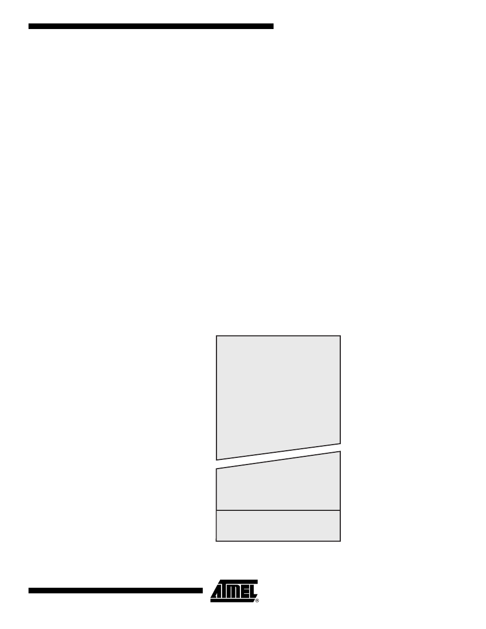
Figure 9. Program Memory Map
0x0000
0x3FFF/0x7FFF
Program Memory
Application Flash Section
Boot Flash Section