Rainbow Electronics ATmega3290P_V User Manual
Page 307
307
ATmega329/3290/649/6490
2552H–AVR–11/06
Notes:
1. This command sequence is not required if the seven MSB are correctly set by the previous command sequence (which is
normally the case).
2. Repeat until o = “1”.
3. Set bits to “0” to program the corresponding Fuse, “1” to unprogram the Fuse.
4. Set bits to “0” to program the corresponding Lock bit, “1” to leave the Lock bit unchanged.
5. “0” = programmed, “1” = unprogrammed.
6. The bit mapping for Fuses Extended byte is listed in Table 125 on page 282
7. The bit mapping for Fuses High byte is listed in Table 126 on page 283
8. The bit mapping for Fuses Low byte is listed in Table 127 on page 283
9. The bit mapping for Lock bits byte is listed in Table 123 on page 281
10. Address bits exceeding PCMSB and EEAMSB (Table 132 and Table 133) are don’t care
11. All TDI and TDO sequences are represented by binary digits (0b...).
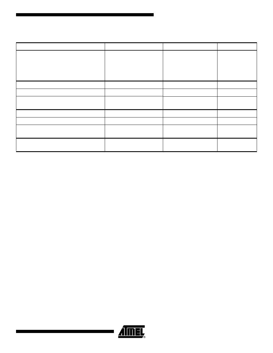
8f. Read Fuses and Lock Bits
0111010_00000000
0111110_00000000
0110010_00000000
0110110_00000000
0110111_00000000
xxxxxxx_xxxxxxxx
xxxxxxx_oooooooo
xxxxxxx_oooooooo
xxxxxxx_oooooooo
xxxxxxx_oooooooo
(5)
Fuse Ext. byte
Fuse High byte
Fuse Low byte
Lock bits
9a. Enter Signature Byte Read
0100011_00001000
xxxxxxx_xxxxxxxx
9b. Load Address Byte
0000011_bbbbbbbb
xxxxxxx_xxxxxxxx
9c. Read Signature Byte
0110010_00000000
0110011_00000000
xxxxxxx_xxxxxxxx
xxxxxxx_oooooooo
10a. Enter Calibration Byte Read
0100011_00001000
xxxxxxx_xxxxxxxx
10b. Load Address Byte
0000011_bbbbbbbb
xxxxxxx_xxxxxxxx
10c. Read Calibration Byte
0110110_00000000
0110111_00000000
xxxxxxx_xxxxxxxx
xxxxxxx_oooooooo
11a. Load No Operation Command
0100011_00000000
0110011_00000000
xxxxxxx_xxxxxxxx
xxxxxxx_xxxxxxxx
Table 138. JTAG Programming Instruction Set (Continued)
a = address high bits, b = address low bits, H = 0 - Low byte, 1 - High Byte, o = data out, i = data in, x = don’t care
Instruction
TDI Sequence
TDO Sequence
Notes