Rainbow Electronics ATmega3290P_V User Manual
Page 314
314
ATmega329/3290/649/6490
2552H–AVR–11/06
Note:
1. “Max” means the highest value where the pin is guaranteed to be read as low
2. “Min” means the lowest value where the pin is guaranteed to be read as high
3. Although each I/O port can sink more than the test conditions (20 mA at V
CC
= 5V, 10 mA at V
CC
= 3V for Port B and 10 mA
at V
CC
= 5V, 5 mA at V
CC
= 3V for all other ports) under steady state conditions (non-transient), the following must be
observed:
TQFP and QFN/MLF Package:
1] The sum of all IOL, for all ports, should not exceed 400 mA.
2] The sum of all IOL, for ports A0 - A7, C4 - C7, G2 should not exceed 100 mA.
3] The sum of all IOL, for ports B0 - B7, E0 - E7, G3 - G5 should not exceed 100 mA.
4] The sum of all IOL, for ports D0 - D7, C0 - C3, G0 - G1 should not exceed 100 mA.
5] The sum of all IOL, for ports F0 - F7, should not exceed 100 mA.
If IOL exceeds the test condition, VOL may exceed the related specification. Pins are not guaranteed to sink current greater
than the listed test condition.
4. Although each I/O port can source more than the test conditions (20 mA at V
CC
= 5V, 10 mA at V
CC
= 3V for Port B and 10mA
at V
CC
= 5V, 5 mA at V
CC
= 3V for all other ports) under steady state conditions (non-transient), the following must be
observed:
TQFP and QFN/MLF Package:
1] The sum of all IOL, for all ports, should not exceed 400 mA.
2] The sum of all IOL, for ports A0 - A7, C4 - C7, G2 should not exceed 100 mA.
3] The sum of all IOL, for ports B0 - B7, E0 - E7, G3 - G5 should not exceed 100 mA.
4] The sum of all IOL, for ports D0 - D7, C0 - C3, G0 - G1 should not exceed 100 mA.
5] The sum of all IOL, for ports F0 - F7, should not exceed 100 mA.
If IOH exceeds the test condition, VOH may exceed the related specification. Pins are not guaranteed to source current
greater than the listed test condition.
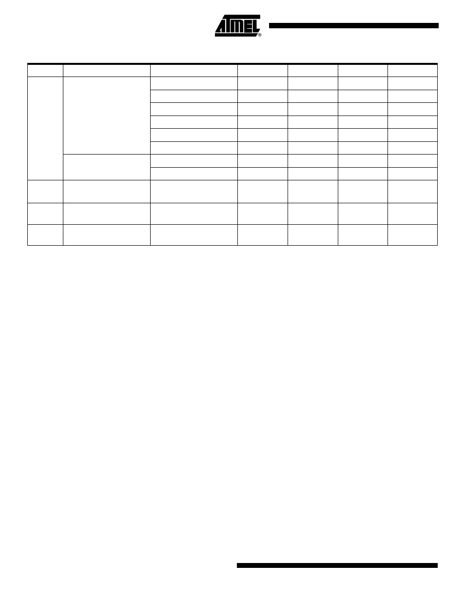
5. Typical values at 25
°C.
I
CC
Power Supply Current
Active 1MHz, V
CC
= 2V
1.5
mA
Active 4MHz, V
CC
= 3V
3.5
mA
Active 8MHz, V
CC
= 5V
12
mA
Idle 1MHz, V
CC
= 2V
0.45
mA
Idle 4MHz, V
CC
= 3V
1.5
mA
Idle 8MHz, V
CC
= 5V
5.5
mA
Power-down mode
WDT enabled, V
CC
= 3V
7
15
µA
WDT disabled, V
CC
= 3V
0.25
2
µA
V
ACIO
Analog Comparator
Input Offset Voltage
V
CC
= 5V
V
in
= V
CC
/2
<10
40
mV
I
ACLK
Analog Comparator
Input Leakage Current
V
CC
= 5V
V
in
= V
CC
/2
-50
50
nA
t
ACID
Analog Comparator
Propagation Delay
V
CC
= 2.7V
V
CC
= 4.0V
750
500
ns
T
A
= -40
°C to 85°C, V
CC
= 1.8V to 5.5V (unless otherwise noted) (Continued)
Symbol
Parameter
Condition
Min.
Typ.
Max.
Units