Register description for i/o-ports, Porta - port a data register, Ddra - port a data direction register – Rainbow Electronics ATmega3290P_V User Manual
Page 86: Pina - port a input pins address, Portb - port b data register, Ddrb - port b data direction register, Pinb - port b input pins address, Portc - port c data register, Ddrc - port c data direction register, Pinc - port c input pins address
86
ATmega329/3210/649/6410
2552H–AVR–11/06
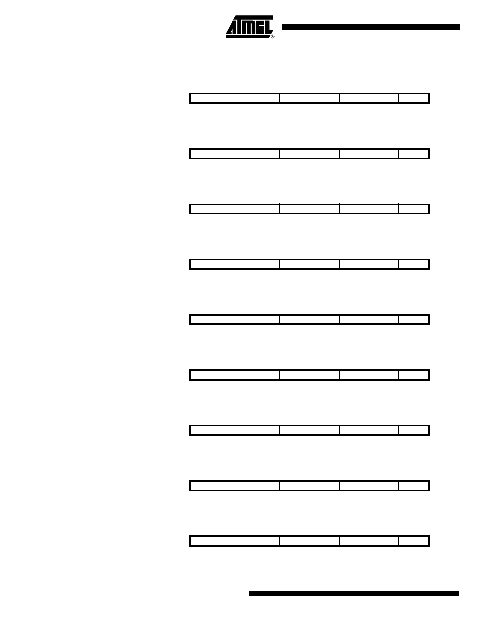
Register Description for I/O-Ports
PORTA – Port A Data Register
DDRA – Port A Data Direction
Register
PINA – Port A Input Pins
Address
PORTB – Port B Data Register
DDRB – Port B Data Direction
Register
PINB – Port B Input Pins
Address
PORTC – Port C Data Register
DDRC – Port C Data Direction
Register
PINC – Port C Input Pins
Address
Bit
7
6
5
4
3
2
1
0
PORTA7
PORTA6
PORTA5
PORTA4
PORTA3
PORTA2
PORTA1
PORTA0
PORTA
Read/Write
R/W
R/W
R/W
R/W
R/W
R/W
R/W
R/W
Initial Value
0
0
0
0
0
0
0
0
Bit
7
6
5
4
3
2
1
0
DDA7
DDA6
DDA5
DDA4
DDA3
DDA2
DDA1
DDA0
DDRA
Read/Write
R/W
R/W
R/W
R/W
R/W
R/W
R/W
R/W
Initial Value
0
0
0
0
0
0
0
0
Bit
7
6
5
4
3
2
1
0
PINA7
PINA6
PINA5
PINA4
PINA3
PINA2
PINA1
PINA0
PINA
Read/Write
R/W
R/W
R/W
R/W
R/W
R/W
R/W
R/W
Initial Value
N/A
N/A
N/A
N/A
N/A
N/A
N/A
N/A
Bit
7
6
5
4
3
2
1
0
PORTB7
PORTB6
PORTB5
PORTB4
PORTB3
PORTB2
PORTB1
PORTB0
PORTB
Read/Write
R/W
R/W
R/W
R/W
R/W
R/W
R/W
R/W
Initial Value
0
0
0
0
0
0
0
0
Bit
7
6
5
4
3
2
1
0
DDB7
DDB6
DDB5
DDB4
DDB3
DDB2
DDB1
DDB0
DDRB
Read/Write
R/W
R/W
R/W
R/W
R/W
R/W
R/W
R/W
Initial Value
0
0
0
0
0
0
0
0
Bit
7
6
5
4
3
2
1
0
PINB7
PINB6
PINB5
PINB4
PINB3
PINB2
PINB1
PINB0
PINB
Read/Write
R/W
R/W
R/W
R/W
R/W
R/W
R/W
R/W
Initial Value
N/A
N/A
N/A
N/A
N/A
N/A
N/A
N/A
Bit
7
6
5
4
3
2
1
0
PORTC7
PORTC6
PORTC5
PORTC4
PORTC3
PORTC2
PORTC1
PORTC0
PORTC
Read/Write
R/W
R/W
R/W
R/W
R/W
R/W
R/W
R/W
Initial Value
0
0
0
0
0
0
0
0
Bit
7
6
5
4
3
2
1
0
DDC7
DDC6
DDC5
DDC4
DDC3
DDC2
DDC1
DDC0
DDRC
Read/Write
R/W
R/W
R/W
R/W
R/W
R/W
R/W
R/W
Initial Value
0
0
0
0
0
0
0
0
Bit
7
6
5
4
3
2
1
0
PINC7
PINC6
PINC5
PINC4
PINC3
PINC2
PINC1
PINC0
PINC
Read/Write
R/W
R/W
R/W
R/W
R/W
R/W
R/W
R/W
Initial Value
N/A
N/A
N/A
N/A
N/A
N/A
N/A
N/A