I/o-ports, Introduction – Rainbow Electronics ATmega3290P_V User Manual
Page 59
59
ATmega329/3290/649/6490
2552H–AVR–11/06
I/O-Ports
Introduction
All AVR ports have true Read-Modify-Write functionality when used as general digital
I/O ports. This means that the direction of one port pin can be changed without uninten-
tionally changing the direction of any other pin with the SBI and CBI instructions. The
same applies when changing drive value (if configured as output) or enabling/disabling
of pull-up resistors (if configured as input). Each output buffer has symmetrical drive
characteristics with both high sink and source capability. Port B has a higher pin driver
strength than the other ports, but all the pin drivers are strong enough to drive LED dis-
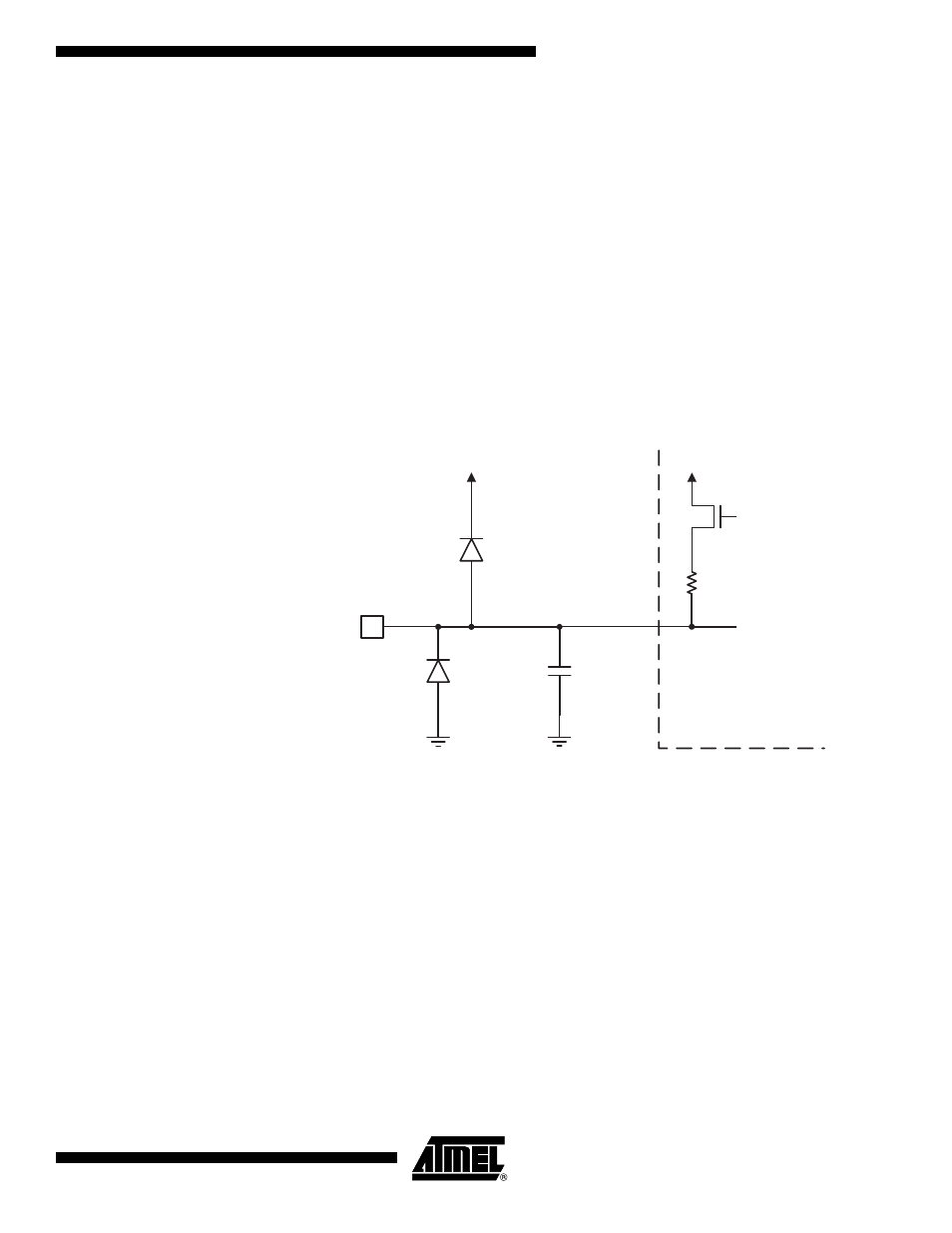
plays directly. All port pins have individually selectable pull-up resistors with a supply-
voltage invariant resistance. All I/O pins have protection diodes to both V
CC
and Ground
as indicated in Figure 23. Refer to “Electrical Characteristics” on page 313 for a com-
plete list of parameters. If exceeding the pin voltage “Absolute Maximum Ratings”,
resulting currents can harm the device if not limited accordingly. For segment pins used
as general I/O, the same situation can also influence the LCD voltage level.
Figure 23. I/O Pin Equivalent Schematic
All registers and bit references in this section are written in general form. A lower case
“x” represents the numbering letter for the port, and a lower case “n” represents the bit
number. However, when using the register or bit defines in a program, the precise form
must be used. For example, PORTB3 for bit no. 3 in Port B, here documented generally
as PORTxn. The physical I/O Registers and bit locations are listed in “Register Descrip-
tion for I/O-Ports” on page 86.
Three I/O memory address locations are allocated for each port, one each for the Data
Register – PORTx, Data Direction Register – DDRx, and the Port Input Pins – PINx. The
Port Input Pins I/O location is read only, while the Data Register and the Data Direction
Register are read/write. However, writing a logic one to a bit in the PINx Register, will
result in a toggle in the corresponding bit in the Data Register. In addition, the Pull-up
Disable – PUD bit in MCUCR disables the pull-up function for all pins in all ports when
set.
Using the I/O port as General Digital I/O is described in “Ports as General Digital I/O” on
page 60. Most port pins are multiplexed with alternate functions for the peripheral fea-
tures on the device. How each alternate function interferes with the port pin is described
C
pin
Logic
R
pu
See Figure
"General Digital I/O" for
Details
Pxn