Scanning the reset pin – Rainbow Electronics ATmega3290P_V User Manual
Page 248
248
ATmega329/3290/649/6490
2552H–AVR–11/06
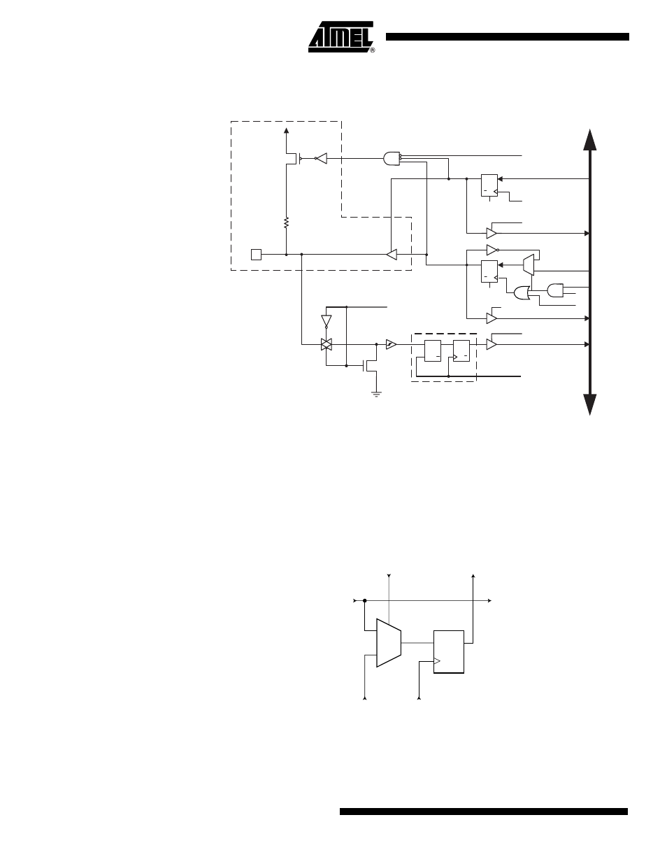
Figure 111. General Port Pin Schematic Diagram
Scanning the RESET Pin
The RESET pin accepts 5V active low logic for standard reset operation, and 12V active
high logic for High Voltage Parallel programming. An observe-only cell as shown in Fig-
ure 112 is inserted both for the 5V reset signal; RSTT, and the 12V reset signal;
RSTHV.
Figure 112. Observe-only Cell
CLK
RPx
RDx
WDx
PUD
SYNCHRONIZER
WDx:
WRITE DDRx
WRx:
WRITE PORTx
RRx:
READ PORTx REGISTER
WPx:
WRITE PINx REGISTER
PUD:
PULLUP DISABLE
CLK :
I/O CLOCK
RDx:
READ DDRx
D
L
Q
Q
RESET
Q
Q
D
Q
Q
D
CLR
DDxn
PINxn
D
ATA
B
U
S
SLEEP
SLEEP:
SLEEP CONTROL
Pxn
I/O
I/O
See Boundary-scan
Description for Details!
PUExn
OCxn
ODxn
IDxn
PUExn:
PULLUP ENABLE for pin Pxn
OCxn:
OUTPUT CONTROL for pin Pxn
ODxn:
OUTPUT DATA to pin Pxn
IDxn:
INPUT DATA from pin Pxn
RPx:
READ PORTx PIN
RRx
RESET
Q
Q
D
CLR
PORTxn
WPx
0
1
WRx
0
1
D
Q
From
Previous
Cell
ClockDR
ShiftDR
To
Next
Cell
From System Pin
To System Logic
FF1
- MAX5151 (16 pages)
- MAXQ3108 (64 pages)
- MAX5661 (39 pages)
- MAX6691 (7 pages)
- MAX5362 (12 pages)
- ADC10158 (26 pages)
- MAX8922L (14 pages)
- MAX8596Z (8 pages)
- MAX7491 (18 pages)
- MAX15040 (15 pages)
- MAX5177 (16 pages)
- ADC08138 (22 pages)
- MAX5961 (42 pages)
- T89C51RD2 (86 pages)
- MAX16055 (9 pages)
- MAX6659 (17 pages)
- ADC0820 (20 pages)
- MAX6678 (19 pages)
- MAX8884Z (15 pages)
- MAX16915 (9 pages)
- MAX8620 (18 pages)
- MAX5144 (12 pages)
- MAX6670 (8 pages)
- MAX8760 (39 pages)
- W78C32C (14 pages)
- MX7533 (8 pages)
- MAX8727 (13 pages)
- MAX9053 (15 pages)
- W78C54 (16 pages)
- MAX8614B (15 pages)
- W90N740 (219 pages)
- MAX6626 (13 pages)
- ADC10738 (30 pages)
- MAX17000 (31 pages)
- MAX5051 (21 pages)
- MAXQ1004 (18 pages)
- MAX6871 (51 pages)
- MX7847 (12 pages)
- MAX6608 (6 pages)
- MAX17083 (15 pages)
- MAX6641 (17 pages)
- MAX5251 (16 pages)
- MAX6338 (8 pages)
- MAX6690 (16 pages)
- MAX8668 (18 pages)