Eearh and eearl - the eeprom address register, Eedr - the eeprom data register, Eecr - the eeprom control register – Rainbow Electronics ATmega3290P_V User Manual
Page 20
20
ATmega329/3290/649/6490
2552H–AVR–11/06
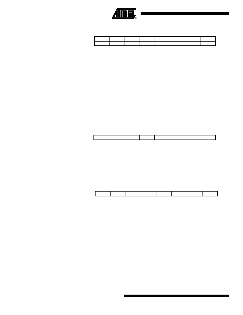
EEARH and EEARL – The
EEPROM Address Register
• Bits 15:11 – Res: Reserved Bits
These bits are reserved bits in the ATmega329/3290/649/6490 and will always read as
zero.
• Bits 10:0 – EEAR10:0: EEPROM Address
The EEPROM Address Registers – EEARH and EEARL specify the EEPROM address
in the 1/2K bytes EEPROM space. The EEPROM data bytes are addressed linearly
between 0 and 1023/2047. The initial value of EEAR is undefined. A proper value must
be written before the EEPROM may be accessed.
Note:
EEAR10 is only valid for ATmega649 and ATmega6490.
EEDR – The EEPROM Data
Register
• Bits 7:0 – EEDR7:0: EEPROM Data
For the EEPROM write operation, the EEDR Register contains the data to be written to
the EEPROM in the address given by the EEAR Register. For the EEPROM read oper-
ation, the EEDR contains the data read out from the EEPROM at the address given by
EEAR.
EECR – The EEPROM Control
Register
• Bits 7:4 – Res: Reserved Bits
These bits are reserved bits in the ATmega329/3290/649/6490 and will always read as
zero.
• Bit 3 – EERIE: EEPROM Ready Interrupt Enable
Writing EERIE to one enables the EEPROM Ready Interrupt if the I bit in SREG is set.
Writing EERIE to zero disables the interrupt. The EEPROM Ready interrupt generates a
constant interrupt when EEWE is cleared.
• Bit 2 – EEMWE: EEPROM Master Write Enable
The EEMWE bit determines whether setting EEWE to one causes the EEPROM to be
written. When EEMWE is set, setting EEWE within four clock cycles will write data to the
EEPROM at the selected address If EEMWE is zero, setting EEWE will have no effect.
When EEMWE has been written to one by software, hardware clears the bit to zero after
four clock cycles. See the description of the EEWE bit for an EEPROM write procedure.
Bit
15
14
13
12
11
10
9
8
–
–
–
–
–
EEAR10
EEAR9
EEAR8
EEARH
EEAR7
EEAR6
EEAR5
EEAR4
EEAR3
EEAR2
EEAR1
EEAR0
EEARL
7
6
5
4
3
2
1
0
Read/Write
R
R
R
R
R
R/W
R/W
R/W
R/W
R/W
R/W
R/W
R/W
R/W
R/W
R/W
Initial Value
0
0
0
0
0
X
X
X
X
X
X
X
X
X
X
X
Bit
7
6
5
4
3
2
1
0
MSB
LSB
EEDR
Read/Write
R/W
R/W
R/W
R/W
R/W
R/W
R/W
R/W
Initial Value
0
0
0
0
0
0
0
0
Bit
7
6
5
4
3
2
1
0
–
–
–
–
EERIE
EEMWE
EEWE
EERE
EECR
Read/Write
R
R
R
R
R/W
R/W
R/W
R/W
Initial Value
0
0
0
0
0
0
X
0