Rainbow Electronics ATmega3290P_V User Manual
Page 252
252
ATmega329/3290/649/6490
2552H–AVR–11/06
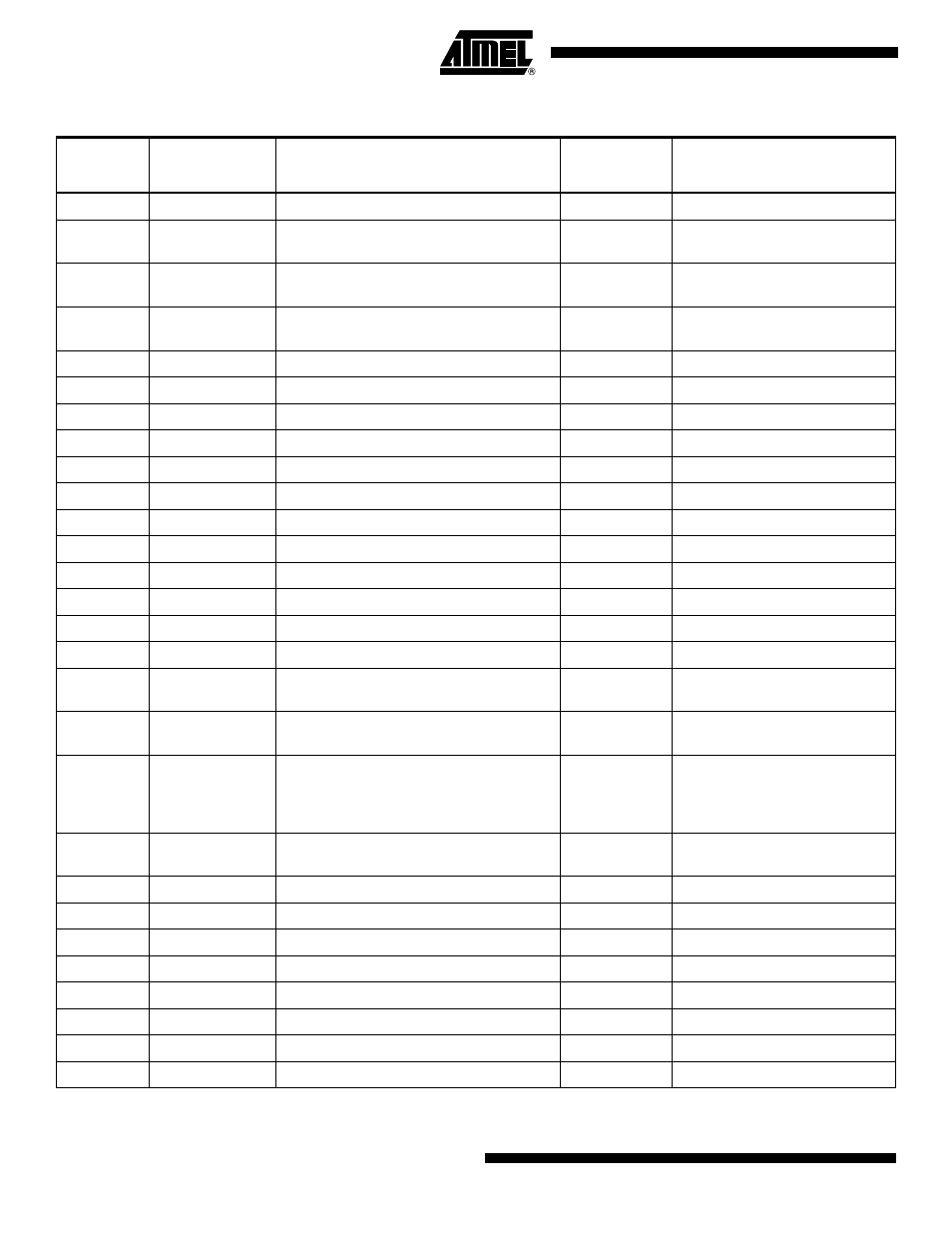
Table 111. Boundary-scan Signals for the ADC
(1)
Signal Name
Direction as seen
from the ADC
Description
Recommended
Input when not
in use
Output Values when
recommended inputs are used,
and CPU is not using the ADC
COMP
Output
Comparator Output
0
0
ACLK
Input
Clock signal to differential amplifier
implemented as Switch-cap filters
0
0
ACTEN
Input
Enable path from differential amplifier to
the comparator
0
0
ADCBGEN
Input
Enable Band-gap reference as negative
input to comparator
0
0
ADCEN
Input
Power-on signal to the ADC
0
0
AMPEN
Input
Power-on signal to the differential amplifier
0
0
DAC_9
Input
Bit 9 of digital value to DAC
1
1
DAC_8
Input
Bit 8 of digital value to DAC
0
0
DAC_7
Input
Bit 7 of digital value to DAC
0
0
DAC_6
Input
Bit 6 of digital value to DAC
0
0
DAC_5
Input
Bit 5 of digital value to DAC
0
0
DAC_4
Input
Bit 4 of digital value to DAC
0
0
DAC_3
Input
Bit 3 of digital value to DAC
0
0
DAC_2
Input
Bit 2 of digital value to DAC
0
0
DAC_1
Input
Bit 1 of digital value to DAC
0
0
DAC_0
Input
Bit 0 of digital value to DAC
0
0
EXTCH
Input
Connect ADC channels 0 - 3 to by-pass
path around differential amplifier
1
1
GNDEN
Input
Ground the negative input to comparator
when true
0
0
HOLD
Input
Sample & Hold signal. Sample analog
signal when low. Hold signal when high. If
differential amplifier are used, this signal
must go active when ACLK is high.
1
1
IREFEN
Input
Enables Band-gap reference as AREF
signal to DAC
0
0
MUXEN_7
Input
Input Mux bit 7
0
0
MUXEN_6
Input
Input Mux bit 6
0
0
MUXEN_5
Input
Input Mux bit 5
0
0
MUXEN_4
Input
Input Mux bit 4
0
0
MUXEN_3
Input
Input Mux bit 3
0
0
MUXEN_2
Input
Input Mux bit 2
0
0
MUXEN_1
Input
Input Mux bit 1
0
0
MUXEN_0
Input
Input Mux bit 0
1
1