Rainbow Electronics ATmega3290P_V User Manual
Page 163
163
ATmega329/3290/649/6490
2552H–AVR–11/06
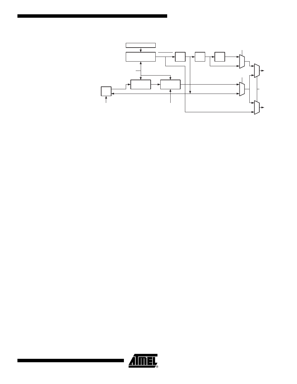
Figure 71. Clock Generation Logic, Block Diagram
Signal description:
txclk
Transmitter clock (Internal Signal).
rxclk
Receiver base clock (Internal Signal).
xcki
Input from XCK pin (internal Signal). Used for synchronous slave operation.
xcko
Clock output to XCK pin (Internal Signal). Used for synchronous master
operation.
fosc
XTAL pin frequency (System Clock).
Internal Clock Generation –
The Baud Rate Generator
Internal clock generation is used for the asynchronous and the synchronous master
modes of operation. The description in this section refers to Figure 71.
The USART Baud Rate Register (UBRRn) and the down-counter connected to it func-
tion as a programmable prescaler or baud rate generator. The down-counter, running at
system clock (f
osc
), is loaded with the UBRRn value each time the counter has counted
down to zero or when the UBRRnL Register is written. A clock is generated each time
the counter reaches zero. This clock is the baud rate generator clock output (=
f
osc
/(UBRRn+1)). The Transmitter divides the baud rate generator clock output by 2, 8 or
16 depending on mode. The baud rate generator output is used directly by the
Receiver’s clock and data recovery units. However, the recovery units use a state
machine that uses 2, 8 or 16 states depending on mode set by the state of the UMSELn,
U2Xn and DDR_XCK bits.
Table 77 contains equations for calculating the baud rate (in bits per second) and for
calculating the UBRRn value for each mode of operation using an internally generated
clock source.
Prescaling
Down-Counter
/2
UBRR
/4
/2
fosc
UBRR+1
Sync
Register
OSC
XCK
Pin
txclk
U2X
UMSEL
DDR_XCK
0
1
0
1
xcki
xcko
DDR_XCK
rxclk
0
1
1
0
Edge
Detector
UCPOL