Rainbow Electronics ATmega3290P_V User Manual
Page 254
254
ATmega329/3290/649/6490
2552H–AVR–11/06
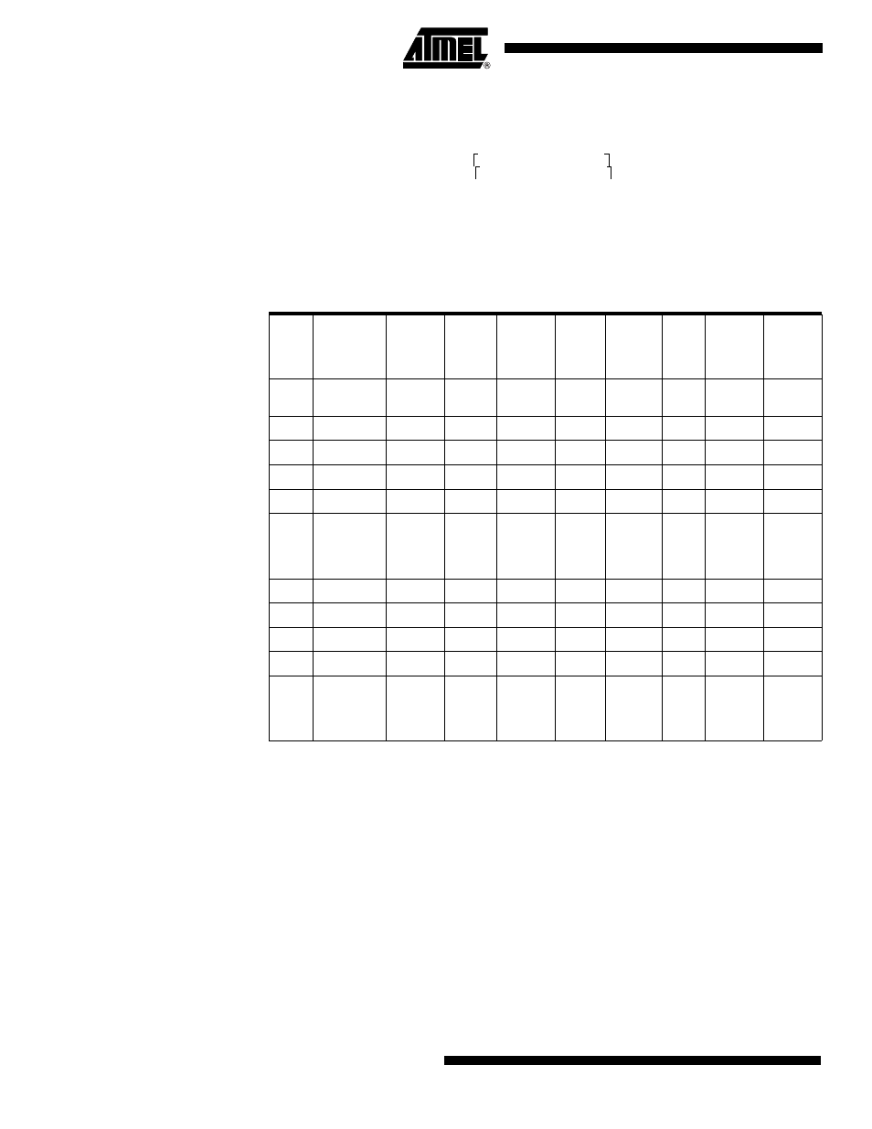
As an example, consider the task of verifying a 1.5V ± 5% input signal at ADC channel 3
when the power supply is 5.0V and AREF is externally connected to V
CC
.
The recommended values from Table 111 are used unless other values are given in the
algorithm in Table 112. Only the DAC and port pin values of the Scan Chain are shown.
The column “Actions” describes what JTAG instruction to be used before filling the
Boundary-scan Register with the succeeding columns. The verification should be done
on the data scanned out when scanning in the data on the same row in the table.
Using this algorithm, the timing constraint on the HOLD signal constrains the TCK clock
frequency. As the algorithm keeps HOLD high for five steps, the TCK clock frequency
has to be at least five times the number of scan bits divided by the maximum hold time,
t
hold,max
Table 112. Algorithm for Using the ADC
Step
Actions
ADCEN
DAC
MUXEN
HOLD
PRECH
PA3.
Data
PA3.
Control
PA3.
Pull-
up_
Enable
1
SAMPLE_
PRELOAD
1
0x200
0x08
1
1
0
0
0
2
EXTEST
1
0x200
0x08
0
1
0
0
0
3
1
0x200
0x08
1
1
0
0
0
4
1
0x123
0x08
1
1
0
0
0
5
1
0x123
0x08
1
0
0
0
0
6
Verify the
COMP bit
scanned
out to be 0
1
0x200
0x08
1
1
0
0
0
7
1
0x200
0x08
0
1
0
0
0
8
1
0x200
0x08
1
1
0
0
0
9
1
0x143
0x08
1
1
0
0
0
10
1
0x143
0x08
1
0
0
0
0
11
Verify the
COMP bit
scanned
out to be 1
1
0x200
0x08
1
1
0
0
0
The lower limit is: 1024 1,5V 0,95 5V
⁄
⋅
⋅
291
0x123
=
=
The upper limit is: 1024 1,5V 1,05 5V
⁄
⋅
⋅
323
0x143
=
=