Spi - serial peripheral interface, Overview, Spi – serial peripheral interface – Rainbow Electronics ATmega3290P_V User Manual
Page 152
152
ATmega329/3290/649/6490
2552H–AVR–11/06
SPI – Serial
Peripheral Interface
The ATmega329/3290/649/6490 SPI includes the following features:
•
Full-duplex, Three-wire Synchronous Data Transfer
•
Master or Slave Operation
•
LSB First or MSB First Data Transfer
•
Seven Programmable Bit Rates
•
End of Transmission Interrupt Flag
•
Write Collision Flag Protection
•
Wake-up from Idle Mode
•
Double Speed (CK/2) Master SPI Mode
Overview
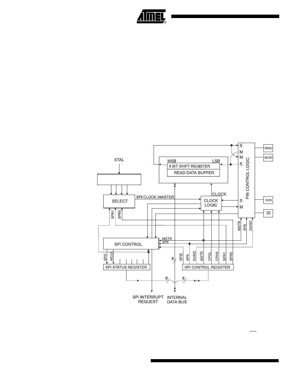
The Serial Peripheral Interface (SPI) allows high-speed synchronous data transfer
between the ATmega329/3290/649/6490 and peripheral devices or between several
AVR devices. A simplified block diagram of the Serial Peripheral Interface is shown in
Figure 66.
The PRSPI bit in “Power Reduction Register” on page 35 must be written to zero to
enable the SPI module.
Figure 66. SPI Block Diagram
(1)
Note:
1. Refer to Figure 1 on page 2, and Table 30 on page 68 for SPI pin placement.
The interconnection between Master and Slave CPUs with SPI is shown in Figure 67.
The system consists of two shift Registers, and a Master clock generator. The SPI Mas-
ter initiates the communication cycle when pulling low the Slave Select SS pin of the
desired Slave. Master and Slave prepare the data to be sent in their respective shift
Registers, and the Master generates the required clock pulses on the SCK line to inter-
SPI2X
SPI2X
DIVIDER
/2/4/8/16/32/64/128