Pcmsk2 - pin change mask register 2(1), Pcmsk1 - pin change mask register 1, Pcmsk0 - pin change mask register 0 – Rainbow Electronics ATmega3290P_V User Manual
Page 58: Pcmsk2 – pin change mask register 2
58
ATmega329/3290/649/6490
2552H–AVR–11/06
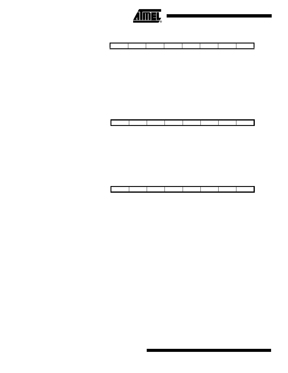
PCMSK2 – Pin Change Mask
Register 2
• Bit 7:0 – PCINT23:16: Pin Change Enable Mask 23:16
Each PCINT23:16 bit selects whether pin change interrupt is enabled on the corre-
sponding I/O pin. If PCINT23:16 is set and the PCIE2 bit in EIMSK is set, pin change
interrupt is enabled on the corresponding I/O pin. If PCINT23:16 is cleared, pin change
interrupt on the corresponding I/O pin is disabled.
Note:
1. PCMSK3 and PCMSK2 are only present in ATmega3290/6490.
PCMSK1 – Pin Change Mask
Register 1
• Bit 7:0 – PCINT15:8: Pin Change Enable Mask 15:8
Each PCINT15:8-bit selects whether pin change interrupt is enabled on the correspond-
ing I/O pin. If PCINT15:8 is set and the PCIE1 bit in EIMSK is set, pin change interrupt is
enabled on the corresponding I/O pin. If PCINT15:8 is cleared, pin change interrupt on
the corresponding I/O pin is disabled.
PCMSK0 – Pin Change Mask
Register 0
• Bit 7:0 – PCINT7:0: Pin Change Enable Mask 7:0
Each PCINT7:0 bit selects whether pin change interrupt is enabled on the correspond-
ing I/O pin. If PCINT7:0 is set and the PCIE0 bit in EIMSK is set, pin change interrupt is
enabled on the corresponding I/O pin. If PCINT7:0 is cleared, pin change interrupt on
the corresponding I/O pin is disabled.
Bit
7
6
5
4
3
2
1
0
PCINT23
PCINT22
PCINT21
PCINT20
PCINT19
PCINT18
PCINT17
PCINT16
PCMSK2
Read/Write
R/W
R/W
R/W
R/W
R/W
R/W
R/W
R/W
Initial
Value
0
0
0
0
0
0
0
0
Bit
7
6
5
4
3
2
1
0
PCINT15
PCINT14
PCINT13
PCINT12
PCINT11
PCINT10
PCINT9
PCINT8
PCMSK1
Read/Write
R/W
R/W
R/W
R/W
R/W
R/W
R/W
R/W
Initial Value
0
0
0
0
0
0
0
0
Bit
7
6
5
4
3
2
1
0
PCINT7
PCINT6
PCINT5
PCINT4
PCINT3
PCINT2
PCINT1
PCINT0
PCMSK0
Read/Write
R/W
R/W
R/W
R/W
R/W
R/W
R/W
R/W
Initial Value
0
0
0
0
0
0
0
0