Clock output buffer, Timer/counter oscillator, System clock prescaler – Rainbow Electronics ATmega3290P_V User Manual
Page 31: Clkpr - clock prescale register
31
ATmega329/3290/649/6490
2552H–AVR–11/06
Clock Output Buffer
When the CKOUT Fuse is programmed, the system Clock will be output on CLKO. This
mode is suitable when the chip clock is used to drive other circuits on the system. The
clock will be output also during reset and the normal operation of I/O pin will be overrid-
den when the fuse is programmed. Any clock source, including internal RC Oscillator,
can be selected when CLKO serves as clock output. If the System Clock Prescaler is
used, it is the divided system clock that is output when the CKOUT Fuse is
programmed.
Timer/Counter Oscillator
ATmega329/3290/649/6490 share the Timer/Counter Oscillator Pins (TOSC1 and
TOSC2) with XTAL1 and XTAL2. This means that the Timer/Counter Oscillator can only
be used when the calibrated internal RC Oscillator is selected as system clock source.
The Oscillator is optimized for use with a 32.768 kHz watch crystal. See Figure 13 on
page 27 for crystal connection.
Applying an external clock source to TOSC1 can be done if EXTCLK in the ASSR Reg-
ister is written to logic one. See “Asynchronous operation of the Timer/Counter” on page
147 for further description on selecting external clock as input instead of a 32 kHz
crystal.
System Clock Prescaler
The ATmega329/3290/649/6490 system clock can be divided by setting the Clock Pres-
cale Register – CLKPR. This feature can be used to decrease power consumption when
the requirement for processing power is low. This can be used with all clock source
options, and it will affect the clock frequency of the CPU and all synchronous peripher-
als. clk
I/O
, clk
ADC
, clk
CPU
, and clk
FLASH
are divided by a factor as shown in Table 13.
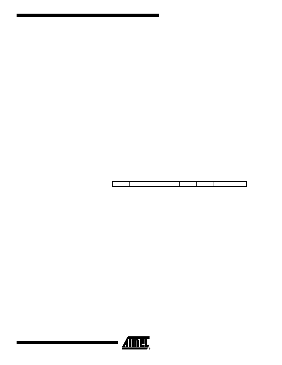
CLKPR – Clock Prescale
Register
• Bit 7 – CLKPCE: Clock Prescaler Change Enable
The CLKPCE bit must be written to logic one to enable change of the CLKPS bits. The
CLKPCE bit is only updated when the other bits in CLKPR are simultaneously written to
zero. CLKPCE is cleared by hardware four cycles after it is written or when CLKPS bits
are written. Rewriting the CLKPCE bit within this time-out period does neither extend the
time-out period, nor clear the CLKPCE bit.
• Bits 3:0 – CLKPS3:0: Clock Prescaler Select Bits 3 - 0
These bits define the division factor between the selected clock source and the internal
system clock. These bits can be written run-time to vary the clock frequency to suit the
application requirements. As the divider divides the master clock input to the MCU, the
speed of all synchronous peripherals is reduced when a division factor is used. The divi-
sion factors are given in Table 13.
To avoid unintentional changes of clock frequency, a special write procedure must be
followed to change the CLKPS bits:
1.
Write the Clock Prescaler Change Enable (CLKPCE) bit to one and all other bits
in CLKPR to zero.
2.
Within four cycles, write the desired value to CLKPS while writing a zero to
CLKPCE.
Interrupts must be disabled when changing prescaler setting to make sure the write pro-
cedure is not interrupted.
Bit
7
6
5
4
3
2
1
0
CLKPCE
–
–
–
CLKPS3
CLKPS2
CLKPS1
CLKPS0
CLKPR
Read/Write
R/W
R
R
R
R/W
R/W
R/W
R/W
Initial Value
0
0
0
0
See Bit Description