Rainbow Electronics W90N740 User Manual
Page 62
W90N740
- 58 -
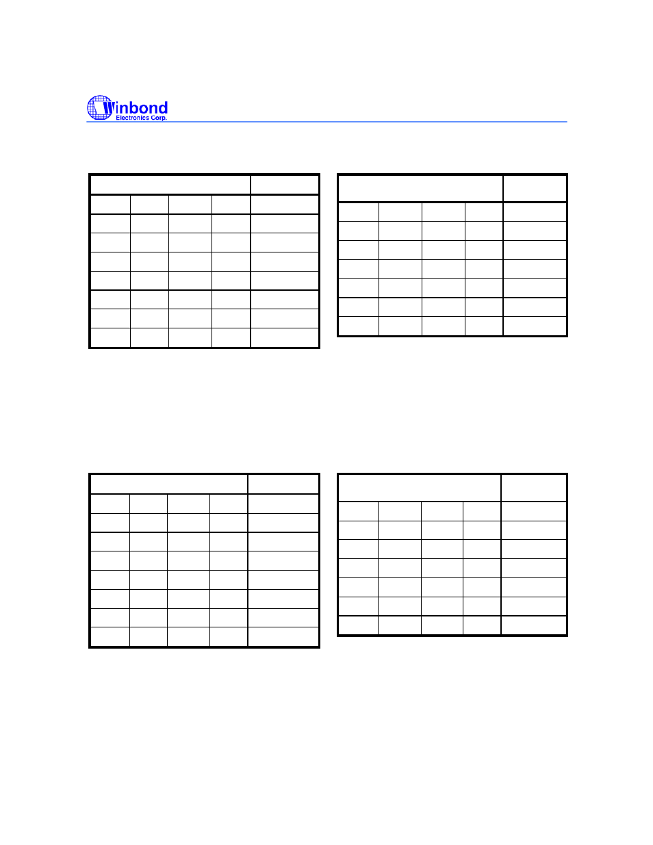
DLH_CLK_SKEW [7:4] :Data latch clock skew adjustment
DLH_CLK_SKEW [7:4]
Gate Delay
0 0 0 0 P-0
0 0 0 1 P-1
0 0 1 0 P-2
0 0 1 1 P-3
0 1 0 0 P-4
0 1 0 1 P-5
0 1 1 0 P-6
0 1 1 1 P-7
DLH_CLK_SKEW [7:4]
Gate
Delay
1 0 0 0 N-0
1 0 0 1 N-1
1 0 1 0 N-2
1 0 1 1 N-3
1 1 0 0 N-4
1 1 0 1 N-5
1 1 1 0 N-6
Note: P-x means Data latched Clock shift “X” gates delays by refer MCLKO positive edge,
N-x means Data latched Clock shift “X” gates delays by refer MCLKO negative edge.
MCLK_O_D [3:0] :MCLK output delay adjustment
MCLK_O_D [3:0]
Gate Delay
0 0 0 0 P-0
0 0 0 1 P-1
0 0 1 0 P-2
0 0 1 1 P-3
0 1 0 0 P-4
0 1 0 1 P-5
0 1 1 0 P-6
0 1 1 1 P-7
MCLK_O_D [3:0]
Gate
Delay
1 0 0 0 N-0
1 0 0 1 N-1
1 0 1 0 N-2
1 0 1 1 N-3
1 1 0 0 N-4
1 1 0 1 N-5
1 1 1 0 N-6
Note: P-x means MCLKO shift “X” gates delay by refer HCLK positive edge,
N-x means MCLKO shift “X” gates delay by refer HCLK negative edge.
MCLK is the output pin of MCLKO, which is a internal signal on chip.