Rainbow Electronics W90N740 User Manual
Page 21
W90N740
Publication Release Date: November 26, 2004
- 17 -
Revision A4
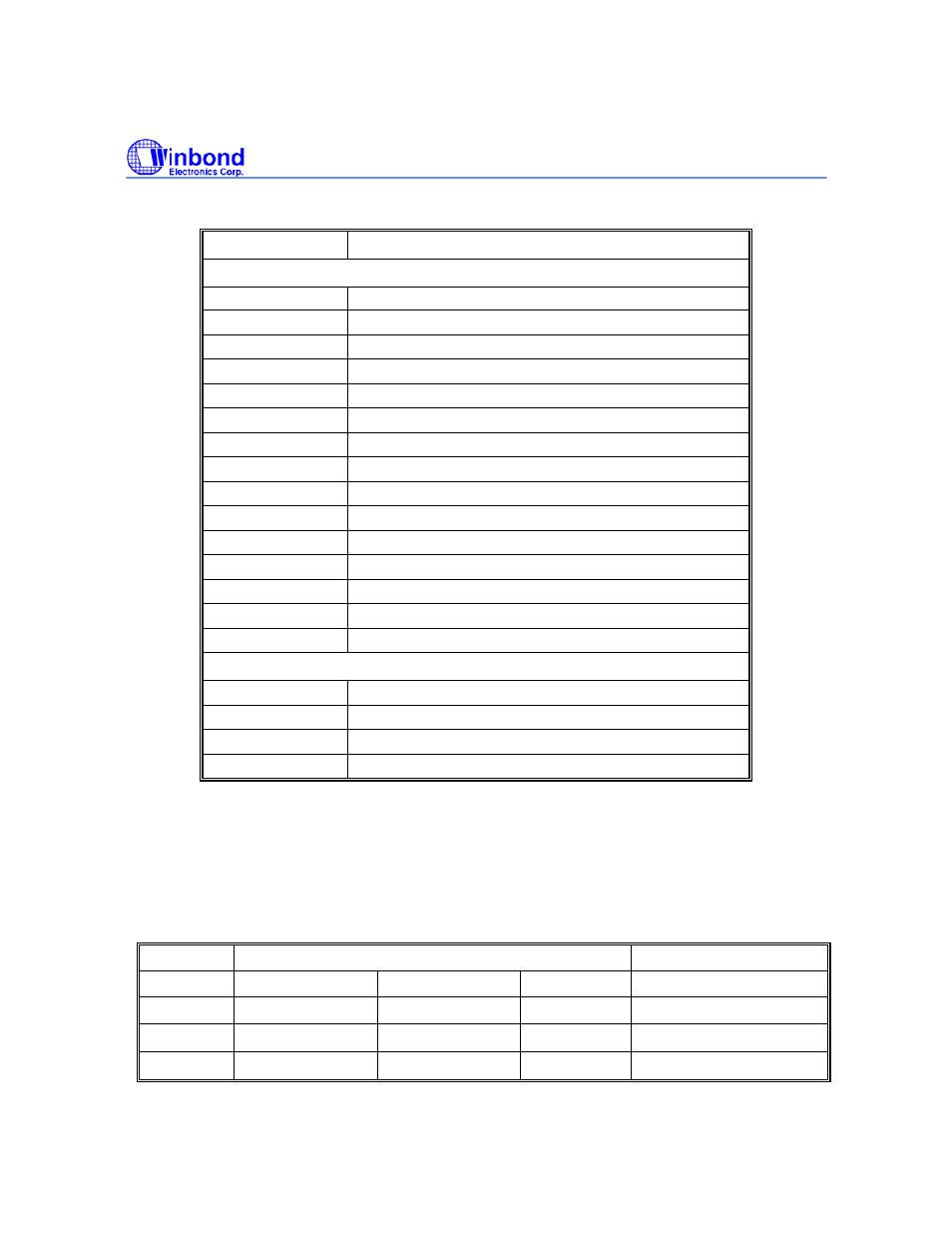
Table 7.2.1 On-Chip Peripherals Memory Map
BASE ADDRESS
DESCRIPTION
AHB Peripherals
0xFFF0.0000 Product
Identifier Register (PDID)
0xFFF0.0004
Arbitration Control Register (ARBCON)
0xFFF0.0008
PLL Control Register (PLLCON)
0xFFF0.000C
Clock Select Register (CLKSEL)
0xFFF0.1000
EBI Control Register (EBICON)
0xFFF0.1004
ROM/FLASH (ROMCON)
0xFFF0.1008
SDRAM bank 0 - 1
0xFFF0.1018
External I/O 0 - 3
0xFFF0.2000
Cache Controller
0xFFF0.3000
Ethernet MAC Controller 0 - 1
0xFFF0.4000
GDMA 0 - 1
0xFFF0.5000
USB (Host)
0xFFF0.6000
NAT Accelerator
0xFFF6.0000
Reserved
0xFFF7.0000
Reserved
APB Peripherals
0xFFF8.0000
UART
0xFFF8.1000
Timer 0 - 1, WDOG Timer
0xFFF8.2000
Interrupt Controller
0xFFF8.3000
GPIO
7.2.3 Address Bus Generation
The W90N740 address bus generation is depended on the required data bus width of each memory
bank. The data bus width is determined by DBWD bits in each bank’s control register.
The maximum accessible memory size of each external IO bank is 32M bytes .
Table 7.2.2 Address Bus Generation Guidelines
DATA BUS
EXTERNAL ADDRESS PINS
MAXIMUM ACCESSIBLE
Width
A [22:0]
A23
A24
Memory Size
8-bit
A22 – A0 (Internal)
A23 (Internal)
A24 (Internal)
32M bytes
16-bit
A23 – A1 (Internal)
A24 (Internal) NA
16M
half-words
32-bit
A24 – A2 (Internal)
NA
NA
8M words