Rainbow Electronics W90N740 User Manual
Page 52
W90N740
- 48 -
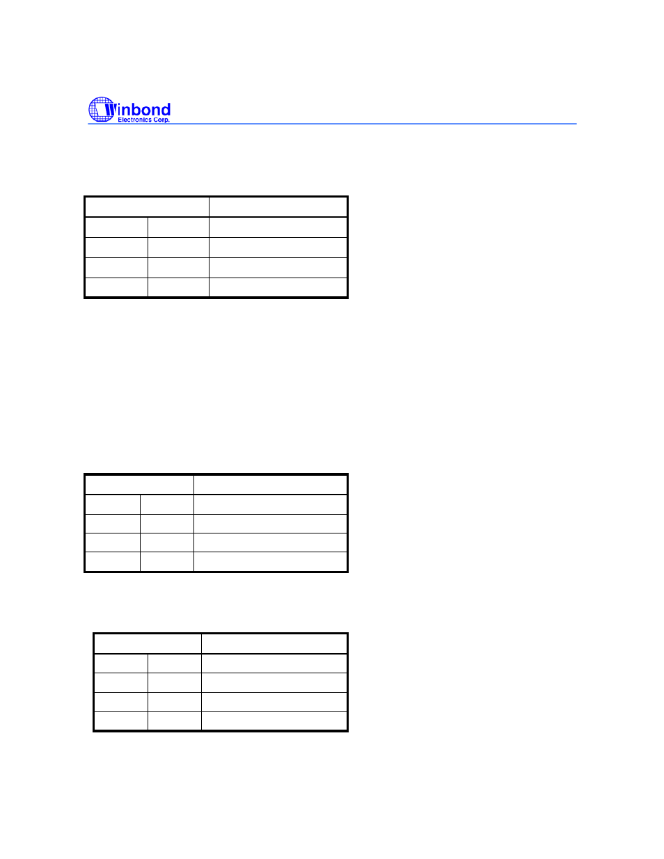
LATENCY [12:11] :The CAS Latency of SDRAM bank 0/1
Defines the CAS latency of external SDRAM bank 0/1
LATENCY [12:11]
MCLK
0 0
1
0 1
2
1 0
3
1 1 REVERSED
COMPBK [7] : Number of component bank in SDRAM bank 0/1
Indicates the number of component bank (2 or 4 banks) in external SDRAM bank 0/1.
0 = 2 banks
1 = 4 banks
DBWD [6:5] :Data bus width for SDRAM bank 0/1
Indicates the external data bus width connect with SDRAM bank 0/1
If DBWD = 00, the assigned SDRAM access signal is not generated i.e. disable.
DBWD [6:5]
Bits
0 0
Bank
disable
0 1
8-bit
(byte)
1 0 16-bit
(half-word)
1 1
32-bit
(word)
COLUMN [4:3] :Number of column address bits in SDRAM bank 0/1
Indicates the number of column address bits in external SDRAM bank 0/1.
COLUMN [4:3]
Bits
0 0
8
0 1
9
1 0
10
1 1
REVERSED
- MAX5151 (16 pages)
- MAXQ3108 (64 pages)
- MAX5661 (39 pages)
- MAX6691 (7 pages)
- MAX5362 (12 pages)
- ADC10158 (26 pages)
- MAX8922L (14 pages)
- MAX8596Z (8 pages)
- MAX7491 (18 pages)
- MAX15040 (15 pages)
- MAX5177 (16 pages)
- ADC08138 (22 pages)
- MAX5961 (42 pages)
- T89C51RD2 (86 pages)
- MAX16055 (9 pages)
- MAX6659 (17 pages)
- ADC0820 (20 pages)
- MAX6678 (19 pages)
- MAX8884Z (15 pages)
- MAX16915 (9 pages)
- MAX8620 (18 pages)
- MAX5144 (12 pages)
- MAX6670 (8 pages)
- MAX8760 (39 pages)
- W78C32C (14 pages)
- MX7533 (8 pages)
- MAX8727 (13 pages)
- MAX9053 (15 pages)
- W78C54 (16 pages)
- MAX8614B (15 pages)
- MAX6626 (13 pages)
- ADC10738 (30 pages)
- MAX17000 (31 pages)
- MAX5051 (21 pages)
- MAXQ1004 (18 pages)
- MAX6871 (51 pages)
- MX7847 (12 pages)
- MAX6608 (6 pages)
- MAX17083 (15 pages)
- MAX6641 (17 pages)
- MAX5251 (16 pages)
- MAX6338 (8 pages)
- MAX6690 (16 pages)
- MAX8668 (18 pages)