No nr nf 1 – Rainbow Electronics W90N740 User Manual
Page 36
W90N740
- 32 -
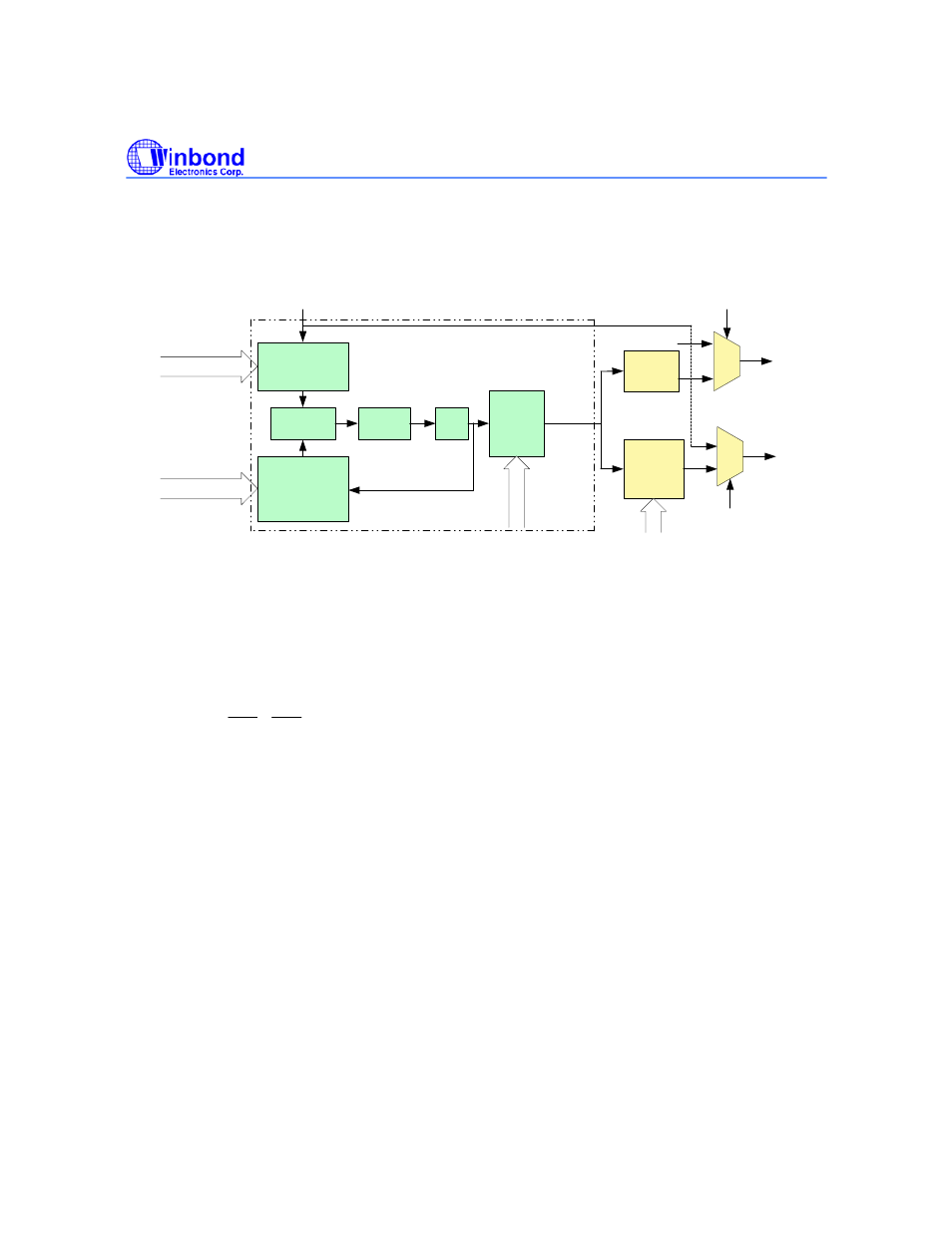
INDV [4:0] :PLL input clock divider
Input Divider divides the input reference clock into the PLL.
Input Divider
(NR)
PFD
Feedback
Divider
(NF)
Charge
Pump
VCO
Output
Divider
(NO)
Clock
Divider
&
Selector
EXTAL
ECLKS
OTDV[1:0]
CLKS[2:0]
1
0
PLL
Internal
System
Clock
INDV[4:0]
FBDV[8:0]
48MHz
Gen
480MHz
0
1
USBCKS
USB
Module
FIN
FOUT
GP12
Fig 7.2.6 System PLL block diagram
The formula of output clock of PLL is:
F
OUT
= F
IN
NO
NR
NF
1
∗
∗
F
OUT:
Output clock of Output Divider
F
IN:
External clock into the Input Divider
NR:Input divider value (NR = INDV + 2)
NF:Feedback divider value (NF = FBDV + 2)
NO:Output divider value (NO = OTDV)
See also other documents in the category Rainbow Electronics Sensors:
- MAX5151 (16 pages)
- MAXQ3108 (64 pages)
- MAX5661 (39 pages)
- MAX6691 (7 pages)
- MAX5362 (12 pages)
- ADC10158 (26 pages)
- MAX8922L (14 pages)
- MAX8596Z (8 pages)
- MAX7491 (18 pages)
- MAX15040 (15 pages)
- MAX5177 (16 pages)
- ADC08138 (22 pages)
- MAX5961 (42 pages)
- T89C51RD2 (86 pages)
- MAX16055 (9 pages)
- MAX6659 (17 pages)
- ADC0820 (20 pages)
- MAX6678 (19 pages)
- MAX8884Z (15 pages)
- MAX16915 (9 pages)
- MAX8620 (18 pages)
- MAX5144 (12 pages)
- MAX6670 (8 pages)
- MAX8760 (39 pages)
- W78C32C (14 pages)
- MX7533 (8 pages)
- MAX8727 (13 pages)
- MAX9053 (15 pages)
- W78C54 (16 pages)
- MAX8614B (15 pages)
- MAX6626 (13 pages)
- ADC10738 (30 pages)
- MAX17000 (31 pages)
- MAX5051 (21 pages)
- MAXQ1004 (18 pages)
- MAX6871 (51 pages)
- MX7847 (12 pages)
- MAX6608 (6 pages)
- MAX17083 (15 pages)
- MAX6641 (17 pages)
- MAX5251 (16 pages)
- MAX6338 (8 pages)
- MAX6690 (16 pages)
- MAX8668 (18 pages)