Rainbow Electronics W90N740 User Manual
Page 164
W90N740
- 160 -
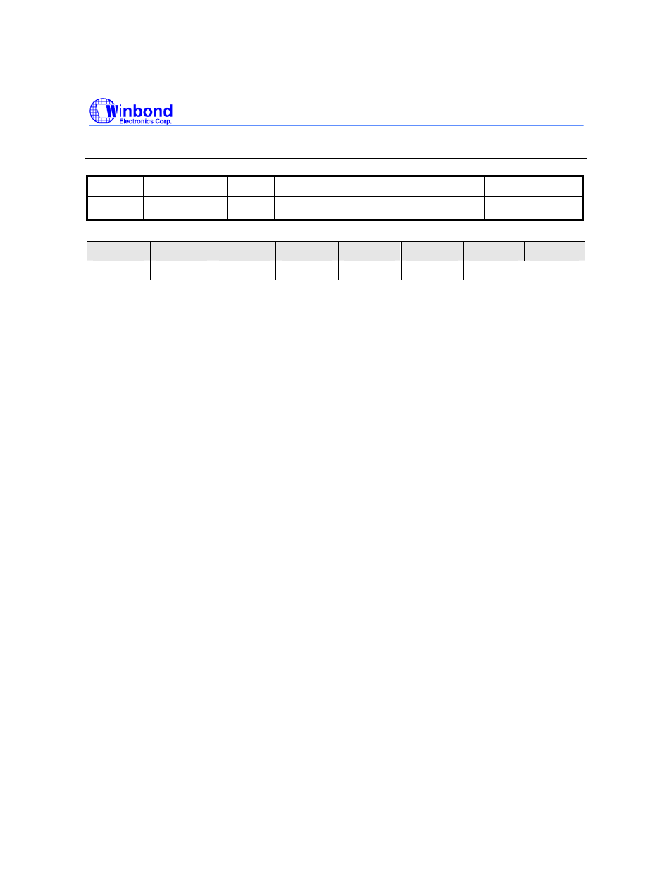
Line Control Register (LCR)
Register Address R/W
Description
Reset
Value
LCR
0xFFF8.000C
R/W Line Control Register
0x0000.0000
7
6
5
4
3
2
1
0
DLAB BCB SPE EPE PBE NSB
WLS
DLAB [7]: Divider Latch Access Bit
0 = It is used to access RBR, THR or IER.
1 = It is used to access Divisor Latch Registers {DLL, DLM}.
BCB [6]: Break Control Bit
When this bit is set to logic 1, the serial data output (SOUT) is forced to the Spacing State (logic 0). This
bit acts only on SOUT and has no effect on the transmitter logic.
SPE [5]: Stick Parity Enable
0 = Disable stick parity
1 = Parity bit is transmitted and checked as a logic 1 if bit 4 is 0 (odd parity), or as a logic 0 if bit 4 is 1
(even parity). This bit has effect only when bit 3 (parity bit enable) is set.
EPE [4]: Even Parity Enable
0 = Odd number of logic 1’s are transmitted or checked in the data word and parity bits.
1 = Even number of logic 1’s are transmitted or checked in the data word and parity bits.
This bit has effect only when bit 3 (parity bit enable) is set.
PBE [3]: Parity Bit Enable
0 = Parity bit is not generated (transmit data) or checked (receive data) during transfer.
1 = Parity bit is generated or checked between the "last data word bit" and "stop bit" of the serial data.
NSB [2]: Number of “STOP bit”
0 = One “ STOP bit” is generated in the transmitted data
1 = One and a half “ STOP bit” is generated in the transmitted data when 5-bit word length is selected;
Two “ STOP bit” is generated when 6-, 7- and 8-bit word length is selected.