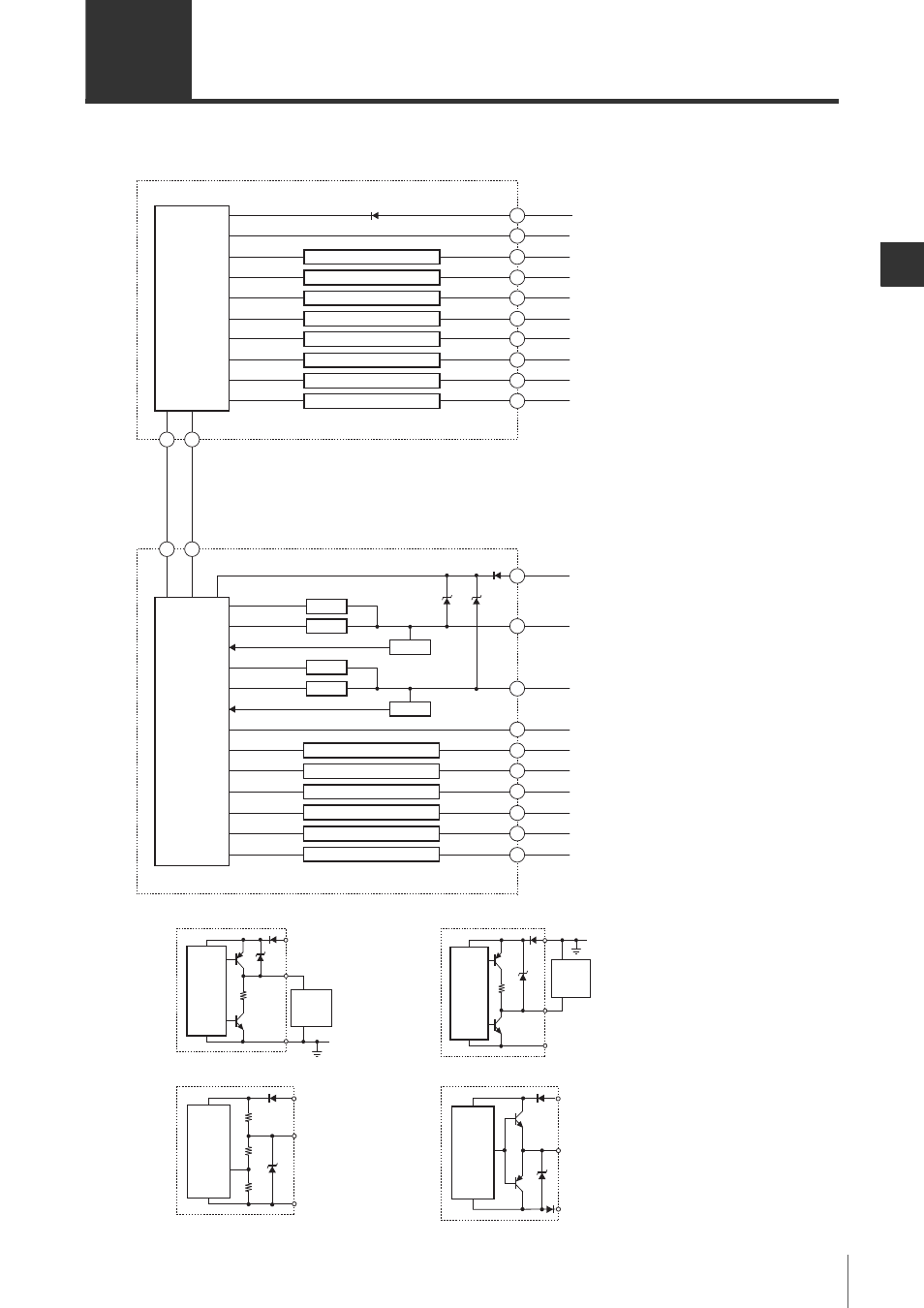
2 i/o circuit diagram, I/o circuit diagram -3, I/o circuit diagram – KEYENCE SL-V Series User Manual
Page 111: Overall circuit diagram

4-3
Wirin
4
SL-V-M-NO4-E
4-2
I/O Circuit Diagram
Overall circuit diagram
Transmitter
Interlock mode selection input circuit
Interlock mode selection input*
1
Brown
+24 V
0 V
Blue
Pink
Violet
Green
Red
Grey
Grey/black
Pink/black
White/black
Wait input circuit
Wait input*
1
*
2
Interlock-reset-ready output circuit
Interlock-reset-ready output
AUX output circuit
AUX
State information output 1 circuit
State information
output 1
State information output 2 circuit
State information
output 2
Alert output circuit
Alert output
Clear/Blocked output circuit
Clear/Blocked output
10
11
12
2
7
1
3
4
8
9
Main circuit
Receiver
Black
OSSD1
White
OSSD2
Brown
+24 V
0 V
Blue
Yellow
Red
Red/black
Yellow/black
Light blue
Light blue/black
Reset input circuit
NPN
PNP
NPN
Reset input
EDM input circuit
EDM input
Override input circuit
Override input*
1
*
2
Muting lamp output circuit
Muting lamp output
Muting input 1
Muting input 1
Muting input 2
Muting input 2
Comm
unication cab
le 2
Comm
unication cab
le 1
Or
ange
Or
ange/b
lac
k
6
5
6
5
2
3
1
7
4
8
9
10
11
12
Monitor
Monitor
Main circuit
PNP
*1 The following changes are
made when muting banks are
being used.
Pink :
Muting bank
input 3
Violet :
Muting bank
input 1
Red/black : Muting bank
input 2
*2 If the center indicator is set to
the Built-in indicator mode,
this is used for the control
input of the indication state.
External
device
Main
circuit
+24 V
0 V
10
OSSD
Ω
10
Ω
External
device
Main
circuit
+24 V
0 V
OSSD
Main
circuit
+24 V
0 V
Input
Output
Main
circuit
+24 V
0 V
OSSD PNP output circuit
OSSD NPN output circuit
Input circuit
Output circuit
