NEC PD78F9488 User Manual
Page 361

CHAPTER 22 ELECTRICAL SPECIFICATIONS (
µ
PD789488, 78F9488, 789489, 78F9489)
User’s Manual U15331EJ4V1UD
361
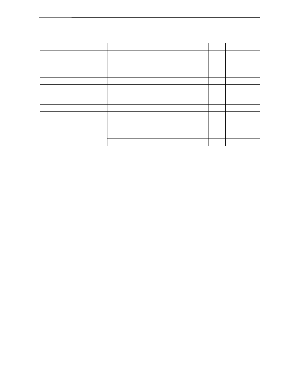
Flash Memory Writing and Erasing Characteristics (T
A
= 10 to 40
°C, V
DD
= 1.8 to 5.5 V)
(
µPD78F9488, 78F9489 only)
Parameter Symbol Conditions MIN.
TYP.
MAX.
Unit
Write/erase operating frequency
f
X
2.7
V
≤ V
DD
≤ 5.5 V
1.0
5
MHz
1.8
V
≤ V
DD
≤ 5.5 V
1.0
1.25
MHz
Write current (V
DD
pin)
Note
I
DDW
When
V
PP
supply voltage = V
PP1
(at 5.0 MHz operation)
7
mA
Write current (V
PP
pin)
Note
I
PPW
When
V
PP
supply voltage = V
PP1
13
mA
Erase current (V
DD
pin)
Note
I
DDE
When
V
PP
supply voltage = V
PP1
(at 5.0 MHz operation)
7
mA
Erase current (V
PP
pin)
Note
I
PPE
When
V
PP
supply voltage = V
PP1
100
mA
Unit erase time
t
er
0.5 1
1
s
Total erase time
t
era
20
s
Number of overwrites
Erase and write is considered as 1
cycle
20
Times
V
PP0
Normal
operation
0
0.2V
DD
V
V
PP
supply voltage
V
PP1
Flash memory programming
9.7
10.0
10.3
V
Note Excludes current flowing through ports (including on-chip pull-up resistors)
