3 10-bit a/d converter control registers – NEC PD78F9488 User Manual
Page 176
CHAPTER 10 10-BIT A/D CONVERTER
176
User’s Manual U15331EJ4V1UD
10.3 10-Bit A/D Converter Control Registers
The 10-bit A/D converter is controlled by the following two registers.
• A/D converter mode register 0 (ADML0)
• Analog input channel specification register 0 (ADS0)
(1) A/D converter mode register 0 (ADML0)
ADML0 specifies the conversion time for analog inputs. It also specifies whether to enable conversion.
ADML0 is set with a 1-bit or 8-bit memory manipulation instruction.
RESET input sets ADML0 to 00H.
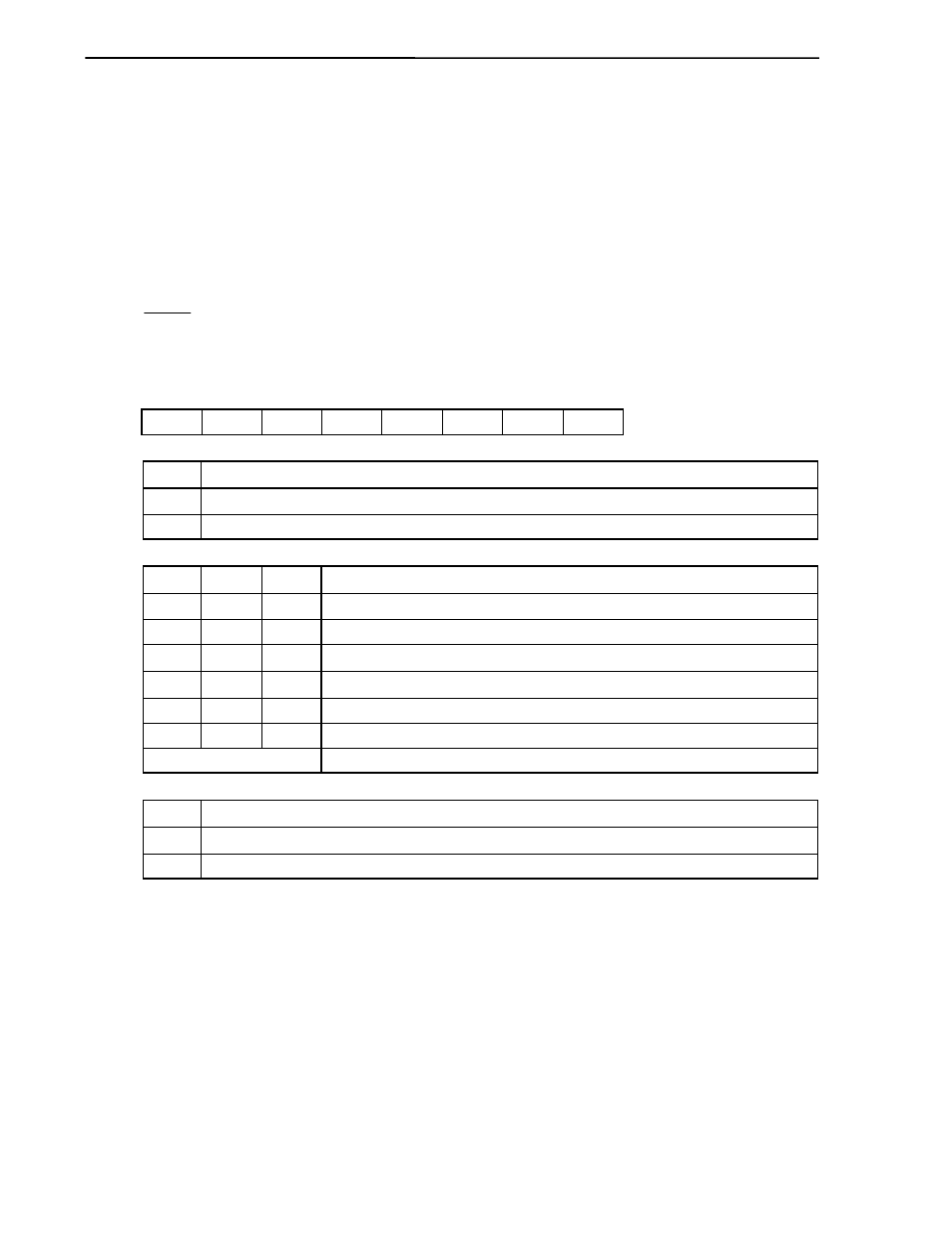
Figure 10-2. Format of A/D Converter Mode Register 0
A/D conversion control
ADCS0
0
1
A/D conversion time selection
Note 1
FR02
0
0
0
1
1
1
144/f
X
120/f
X
96/f
X
72/f
X
60/f
X
48/f
X
FR01
0
0
1
0
0
1
(28.8 s)
(24 s)
(19.2 s)
(14.4 s)
(Setting prohibited
Note 2
)
(Setting prohibited
Note 2
)
µ
µ
µ
FR00
0
1
0
0
1
0
Other than above
Conversion disabled
Conversion enabled
Control of band-gap circuit
ADCE0
0
1
Band-gap circuit stopped
Band-gap circuit operating
Setting prohibited
µ
ADCS0
0
FR02
FR01
FR00
0
0
ADCE0
ADML0
<7>
6
5
4
Symbol
Address
After reset
R/W
FF80H
00H
R/W
3
2
1
0
Notes 1. The specifications of FR02, FR01, and FR00 must be such that the A/D conversion time is at least
14
µs.
2. When f
X
is 5.0 MHz, these bit combinations must not be used, as the A/D conversion time will fall
below 14
µs.