NEC PD78F9488 User Manual
Page 251

CHAPTER 13 LCD CONTROLLER/DRIVER
User’s Manual U15331EJ4V1UD
251
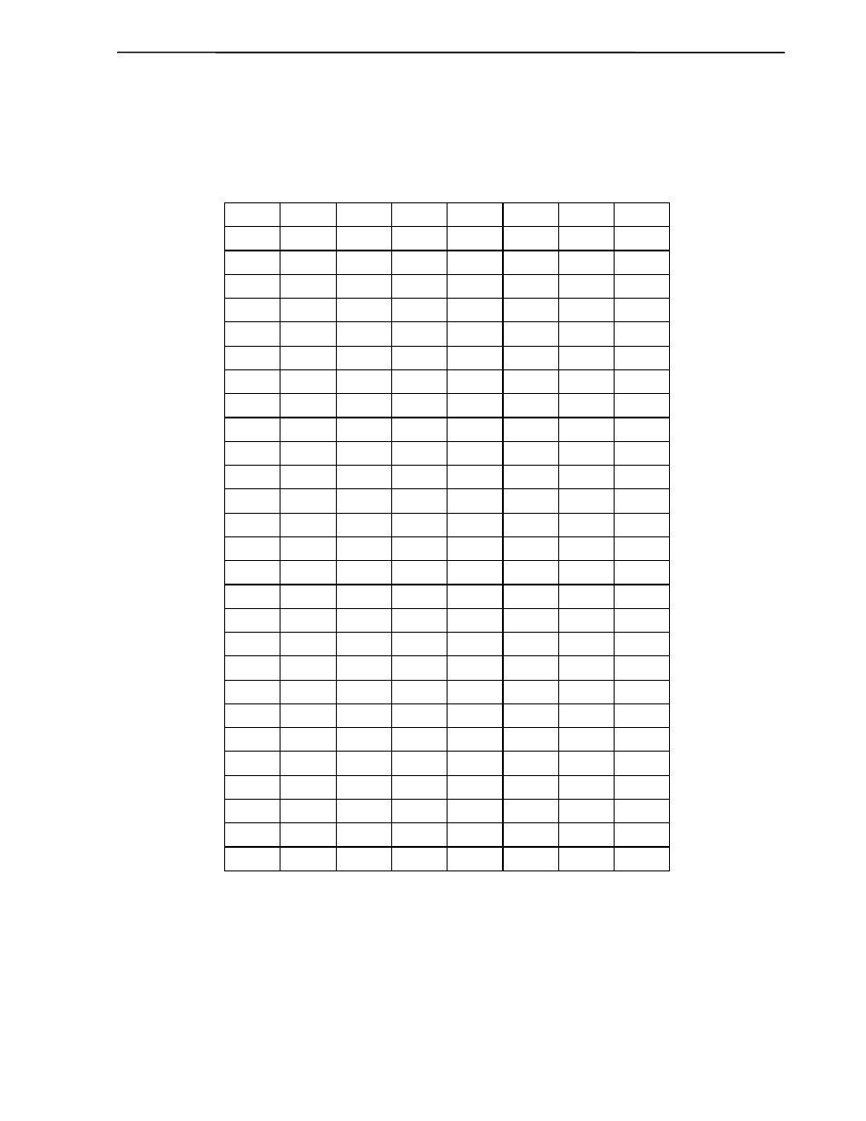
The correspondence with the LCD display RAM is shown in Figure 13-1 below.
Figure 13-1. Correspondence with LCD Display RAM
Address
Bit
Segment
7 6 5 4 3 2 1 0
FA1BH 0 0 0 0
→ S27
Note
FA1AH 0 0 0 0
→ S26
Note
FA19H 0 0 0 0
→ S25
Note
FA18H 0 0 0 0
→ S24
Note
FA17H 0 0 0 0
→ S23
Note
FA16H 0 0 0 0
→ S22
Note
FA15H 0 0 0 0
→ S21
Note
FA14H 0 0 0 0
→ S20
Note
FA13H 0 0 0 0
→ S19
Note
FA12H 0 0 0 0
→ S18
Note
FA11H 0 0 0 0
→ S17
Note
FA10H 0 0 0 0
→ S16
Note
FA0FH 0 0 0 0
→ S15
FA0EH 0 0 0 0
→ S14
FA0DH 0 0 0 0
→ S13
FA0CH 0 0 0 0
→ S12
FA0BH 0 0 0 0
→ S11
FA0AH 0 0 0 0
→ S10
FA09H 0 0 0 0
→ S9
FA08H 0 0 0 0
→ S8
FA07H 0 0 0 0
→ S7
FA06H 0 0 0 0
→ S6
FA05H 0 0 0 0
→ S5
FA04H 0 0 0 0
→ S4
FA03H 0 0 0 0
→ S3
FA02H 0 0 0 0
→ S2
FA01H 0 0 0 0
→ S1
FA00H 0 0 0 0
→ S0
Common
↑
COM3
↑
COM2
↑
COM1
↑
COM0
Note Segments S16 to S27 are selected in 1-bit units via a mask option or port function register (segment
output pin/port pin).
Remark Bits 4 to 7 are fixed to 0.
