NEC PD78F9488 User Manual
Page 229
CHAPTER 12 SERIAL INTERFACE 1A0
User’s Manual U15331EJ4V1UD
229
(3) MSB/LSB switching as the start bit
In the 3-wire serial I/O mode, transfer can be selected to start from the MSB or LSB.
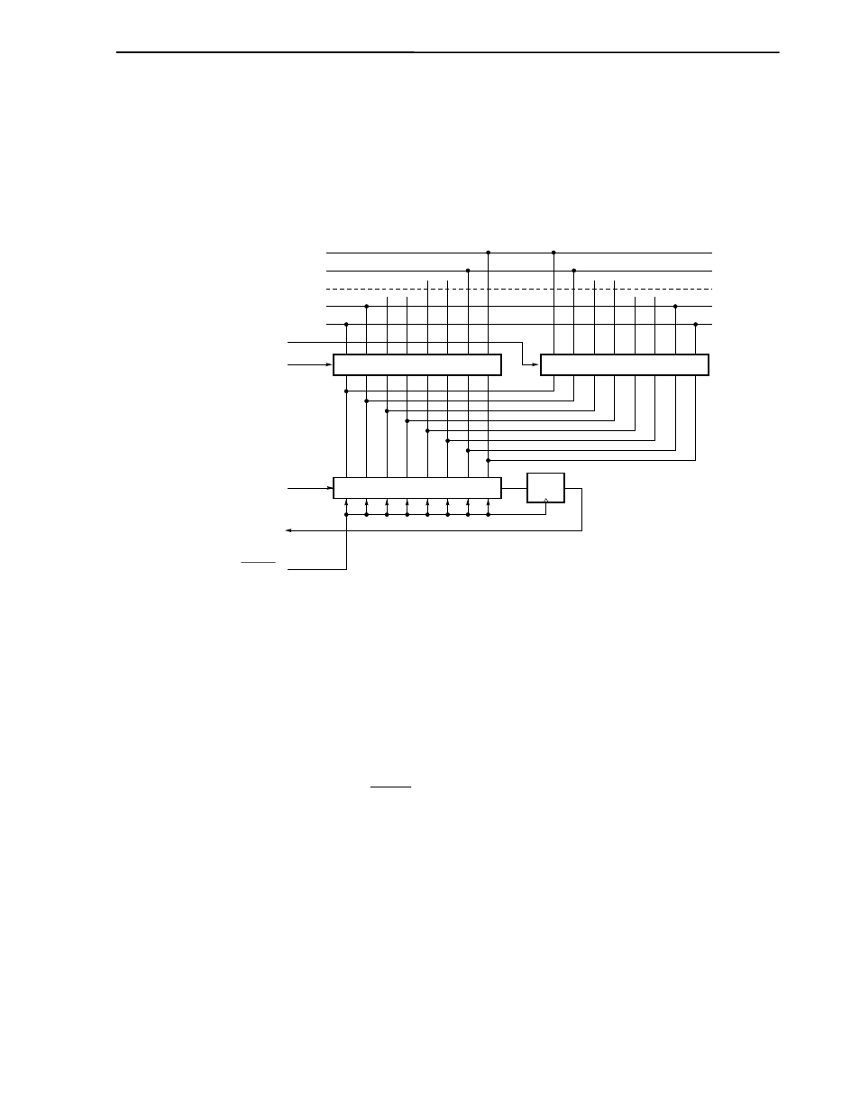
Figure 12-6 shows the configuration of serial I/O shift register 1A0 (SIO1A0) and the internal bus. As shown
in the figure, MSB/LSB can be read/written in reverse form.
MSB/LSB switching as the start bit can be specified with bit 6 (DIR10) of serial operation mode register 1A0
(CSIM1A0).
Figure 12-6. Circuit of Switching in Transfer Bit Order
7
6
Internal bus
1
0
LSB-first
MSB-first
Read/write gate
SI10
Shift I/O shift register 1A0 (SIO1A0)
Read/write gate
SO10
SCK10
D
Q
SO1 latch
Start bit switching is realized by switching the bit order for data write to SIO1A0. The SIO1A0 shift order
remains unchanged.
Thus, switching between MSB-first and LSB-first must be performed before writing data to the shift register.
(4) Transfer
start
Serial transfer is started by setting transfer data to serial I/O shift register 1A0 (SIO1A0) when the following
two conditions are satisfied.
• Bit 7 (CSIE10) of serial operation mode register 1A0 (CSIM1A0) = 1
• Internal serial clock is stopped or SCK10 is high after 8-bit serial transfer.
Caution If CSIE10 is set to “1” after data is written to SIO1A0, transfer does not start.
Termination of 8-bit transfer stops the serial transfer automatically and generates the interrupt request signal
(INTCSI10).