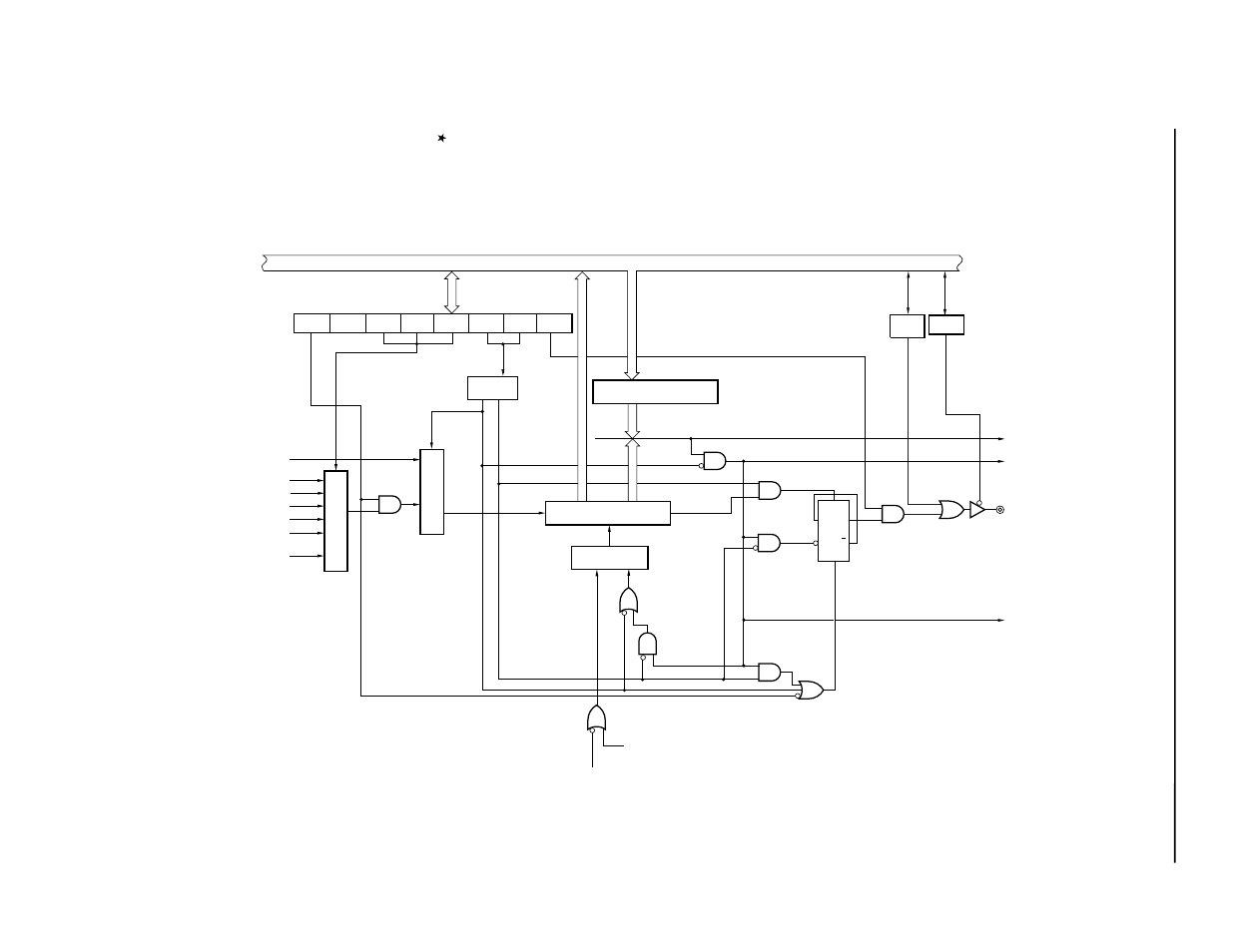
Figure 7-2. block diagram of timer 50 – NEC PD78F9488 User Manual
Page 123
CHA
PTER 7 8-BIT TIMERS 50, 60, A
ND 61
User’s Manual U15331EJ4V1UD
123
Figure 7-2. Block Diagram of Timer 50
TEG50
TCL500
TCL501
8-bit timer mode control register 50
(TMC50)
Decoder
Selector
Selector
8-bit compare register 50
(CR50)
8-bit timer counter 50
(TM50)
Selector
Count operation start signal
from Figure 7-3(D)
(cascade connection)
INTTM50
f
X
/2
3
f
X
/2
7
Timer 60 interrupt request signal
(from Figure 7-3(B))
Carrier clock
(from Figure 7-3(C))
Cascade
connection
mode
Match
Timer 60 match signal
from Figure 7-3(E)
(in cascade connection mode)
Internal bus
OVF
Bit 7 of TM60
(from Figure 7-3(A))
(A)
(B)
(C)
TOE50
P30
output latch
PM30
Timer 50 match signal
to Figure 7-3(F)
(in cascade connection mode)
Timer 50 match signal
to Figure 7-3(G)
(in carrier generator mode)
TO50/TMI60/
INTP0/P30
TCE50
TCL502
f
X
f
XT
TMD500
TMD501
S
Q
IN
R
Q
CK
Clear
PWM mode
(D)
(E)
(F)
(G)