NEC PD78F9488 User Manual
Page 174
CHAPTER 10 10-BIT A/D CONVERTER
174
User’s Manual U15331EJ4V1UD
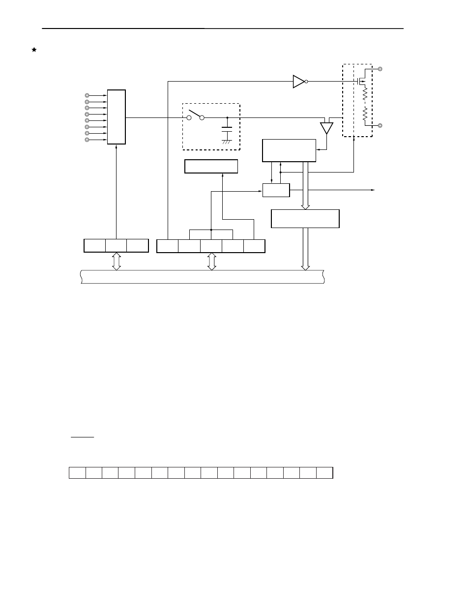
Figure 10-1. Block Diagram of 10-Bit A/D Converter
ANI3/P63
Sample & hold circuit
Voltage comparator
Successive
approximation
register (SAR)
Controller
A/D conversion result
register 0 (ADCRL0)
AV
SS
INTAD0
A/D converter mode
register 0 (ADML0)
Internal bus
V
SS
ADCS0 FR02
FR01
FR00
ADS01
P-ch
AV
DD
Analog input channel
specification register 0
(ADS0)
ADS00
ADS02
ADCE0
ANI2/P62
ANI5/P65
ANI4/P64
ANI1/P61
ANI0/P60
ANI7/P67
ANI6/P66
Selector
Tap selector
Band -gap circuit
(1) Successive approximation register (SAR)
The SAR receives the result of comparing an analog input voltage and a voltage at a voltage tap (comparison
voltage), received from the series resistor string, starting from the most significant bit (MSB).
Upon receiving all the bits, down to the least significant bit (LSB), that is, upon the completion of A/D
conversion, the SAR sends its contents to A/D conversion result register 0 (ADCRL0).
(2) A/D conversion result register 0 (ADCRL0)
ADCRL0 is a 16-bit register that holds the result of A/D conversion. The lower 6 bits are fixed to 0. Each
time A/D conversion ends, the conversion result in the successive approximation register is loaded into
ADCRL0. The results are stored in ADCRL0 from the highest bit.
The higher 8 bits of the conversion result are stored in FF15H and the lower 2 bits of the conversion result
are stored in FF14H.
ADCRL0 can be read with a 16-bit memory manipulation instruction.
RESET input sets ADCRL0 to 0000H.
Symbol
ADCRL0
ADCRL0H (FF15H)
0
0
0
0
0
0
ADCRL0L (FF14H)
FF14H,
FF15H
Address After reset
0000H
R/W
R