4 divider circuit, 5 when subsystem clock is not used, 6 subsystem clock (4 multiplication circuit – NEC PD78F9488 User Manual
Page 104
CHAPTER 5 CLOCK GENERATOR
104
User’s Manual U15331EJ4V1UD
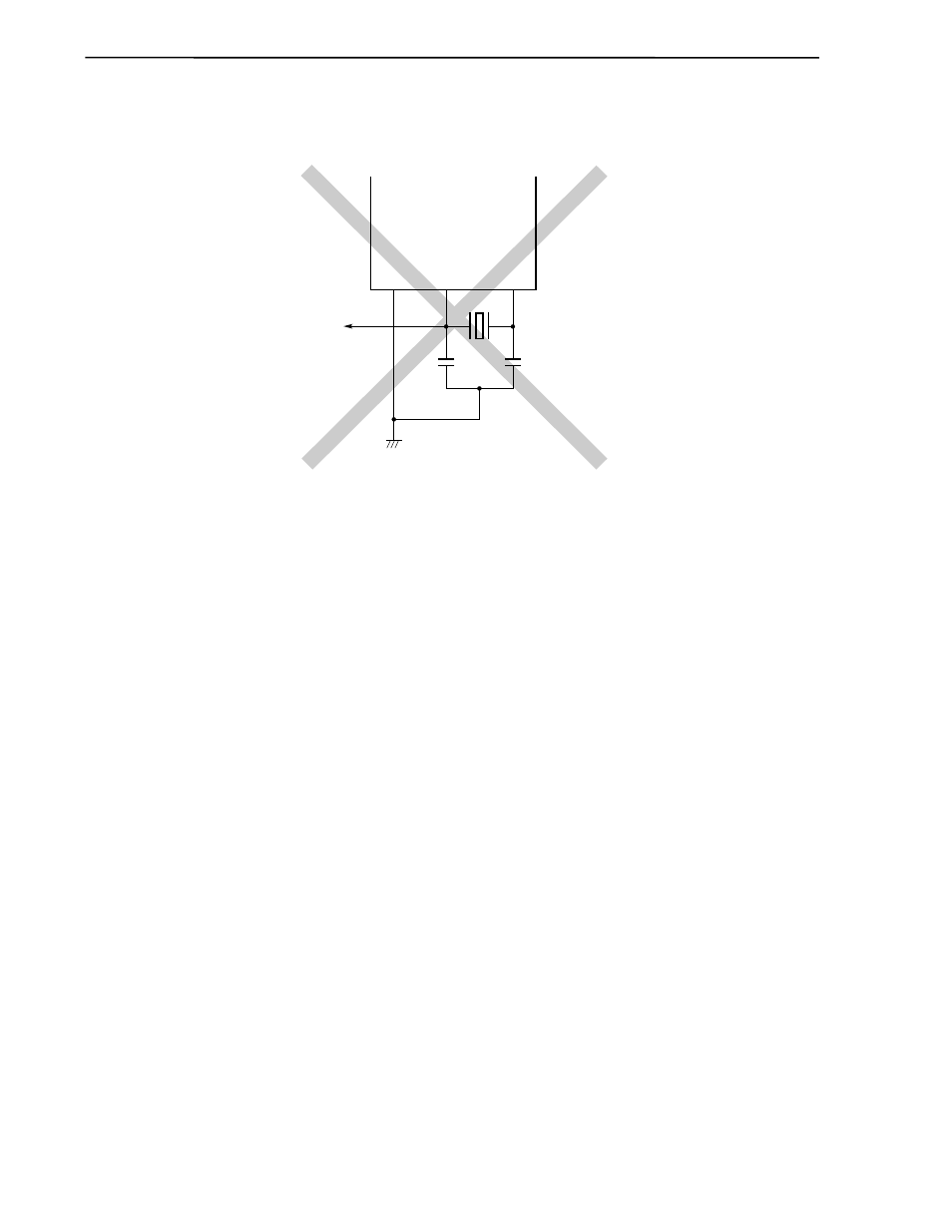
Figure 5-9. Examples of Incorrect Resonator Connection (2/2)
(e) Signal is fetched
V
SS
X1
X2
Remark When using the subsystem clock, read X1 and X2 as XT1 and XT2, respectively, and connect a resistor
to XT2 in series.
5.4.4 Divider circuit
The divider circuit divides the output of the main system clock oscillator (f
X
) to generate various clocks.
5.4.5 When subsystem clock is not used
If the subsystem clock is not necessary, for example, for low-power consumption operation or clock operation,
handle the XT1 and XT2 pins as follows.
XT1: Connect to V
SS
XT2: Leave open
In this case, however, a small current leaks via the on-chip feedback resistor in the subsystem clock oscillator
when the main system clock is stopped. To avoid this, set bit 1 (FRC) of the subclock oscillation mode register
(SCKM) so that the on-chip feedback resistor will not be used. Also in this case, handle the XT1 and XT2 pins as
stated above.
5.4.6 Subsystem clock
×4 multiplication circuit
This circuit multiplies the subsystem clock by 4 and supplies it to the CPU.
The circuit stops operating in the HALT mode (to reduce power consumption).
When the circuit starts operating after HALT mode is released, a one-clock wait of the original subsystem clock is
inserted to eliminate noise.