6 block diagram – NEC PD78F9488 User Manual
Page 34
CHAPTER 1 GENERAL
34
User’s Manual U15331EJ4V1UD
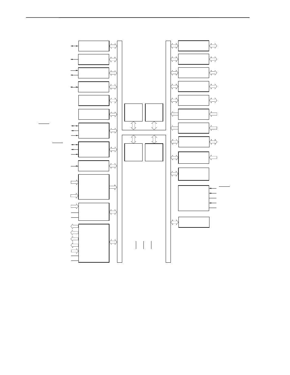
1.6 Block Diagram
78K/0S
CPU core
ROM
(flash
memory)
RAM
V
DD
V
SS
IC0
(V
PP
)
CPT20/TO20/P33
8-bit timer/
event counter 60
P00 to P07
Port 0
P10 to P11
Port 1
P20 to P25
Port 2
P30 to P34
Port 3
P50 to P53
Port 5
P60 to P67
Port 6
P70 to P73
Note 1
Port 7
8-bit timer/
event counter 61
16-bit timer 20
Watch timer
Watchdog timer
Serial
interface 20
TO50/P30
TO60/P31
SCK20/ASCK20/P20
SI20/RxD20/P22
SO20/TxD20/P21
A/D converter
ANI0/P60 to
ANI7/P67
AV
DD
AV
SS
V
LC0
to V
LC2
S0 to S15
COM0 to COM3
LCD
controller/driver
System
control
RESET
X1
X2
XT1
XT2
Interrupt
control
P80 to P87
Note 2
Port 8
Key return
Note 3
KR0/P00 to
KR7/P07
Note 4
KR00/P00 to
KR07/P07
Note 4
KR10/ANI0/P60 to
KR17/ANI7/P67
Standby
control
INTP0/P30 to
INTP3/P33
RAM space
for LCD
data
8-bit timer 50
TMI60/P30
TMI61/TO61/P32
Remote control
signal receiver
Note 4
Note 4
RIN/P34
Serial
interface 1A0
SCK10/P23
SI10/P25
SO10/P24
Note 1
S16 to S19
Note 2
S20 to S27
Multiplier
CAPH
CAPL
Notes 1. Whether to use these pin as input ports (P70 to P73) or segment outputs (S16 to S19) can be selected
in 1-bit units by means of a mask option in the
µPD789488, 789489 or a port mode register in the
µPD78F9488, 78F9489 (refer to 4.3 (3) Port function registers and CHAPTER 20 MASK OPTIONS).
2. Whether to use these pins as I/O port pins (P80 to P87) or segment outputs (S20 to S27) can be
selected in 1-bit units by means of a mask option in the
µPD789488 or a port mode register in the
µPD78F9488, 78F9489 (refer to 4.3 (3) Port function registers and CHAPTER 20 MASK OPTIONS).
3. When
µPD789488, 78F9488 is used.
4. When
µPD789489, 78F9489 is used.
Remark The parenthesized values apply to the flash memory version.