5 cautions related to 10-bit a/d converter – NEC PD78F9488 User Manual
Page 182

CHAPTER 10 10-BIT A/D CONVERTER
182
User’s Manual U15331EJ4V1UD
10.5 Cautions Related to 10-Bit A/D Converter
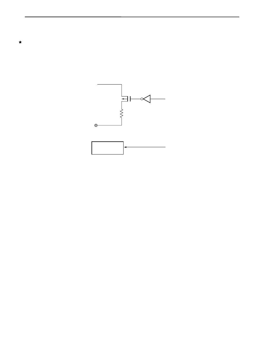
(1) Current consumption in standby mode
In standby mode, the A/D converter stops operation. Clearing bit 7 (ADCS0) and bit 0 (ADCE0) of A/D
converter mode register 0 (ADML0) to 0 can reduce the current consumption.
Figure 10-7 shows how to reduce the current consumption in standby mode.
Figure 10-7. How to Reduce Current Consumption in Standby Mode
AV
REF
V
SS
P-ch
Series resistor string
ADCS0
Band-gap circuit
ADCE0
0: Stopped
1: Operating
(2) Input range for pins ANI0 to ANI7
Be sure to keep the input voltage at ANI0 to ANI7 within the rating. If a voltage greater than or equal to AV
DD
or less than or equal to AV
SS
(even within the absolute maximum ratings) is input into a conversion channel,
the conversion output of the channel becomes undefined, which may affect the conversion output of the other
channels.
(3) Conflict
<1> Conflict between writing to A/D conversion result register 0 (ADCRL0) at the end of conversion and
reading from ADCRL0 using instruction
Reading from ADCRL0 takes precedence. After reading, the new conversion result is written to ADCRL0.
<2> Conflict between writing to ADCRL0 at the end of conversion and writing to A/D converter mode register 0
(ADML0) or analog input channel specification register 0 (ADS0)
Writing to ADML0 or ADS0 takes precedence. ADCRL0 is not written to. No A/D conversion end
interrupt request signal (INTAD0) is generated.
(4) Conversion result immediately after start of A/D conversion
If the band-gap circuit is not used (ADCE0 = 0) or conversion is started before 14
µs has elapsed following
the setting of ADCE, only the first A/D conversion value immediately after A/D conversion has been started is
undefined. Poll the A/D conversion end interrupt request (INTAD0), drop the first conversion result and use
the second and subsequent conversion results. When 14
µs have elapsed following the activation of the
band-gap circuit (ADCE0 = 1), the first conversion value is normal.
