Appendix b, ddr sdram, On the nios development board, cyclone ii edition – Altera DDR SDRAM Controller User Manual
Page 95
© March 2009
Altera Corporation
DDR and DDR2 SDRAM Controller Compiler User Guide
B. DDR SDRAM on the Nios Development
Board, Cyclone II Edition
This appendix walks you through the procedure for using the Altera DDR SDRAM
Controller MegaCore function with the Nios
®
II processor and SOPC Builder. To
ensure that you create a reliable working system, follow these steps:
1. In SOPC Builder, when adding a DDR SDRAM component for a system with the
Nios Development Board, Cyclone
™
II Edition, use the specific IP Toolbench
preset. All other wizard settings are then correct.
1
You may have to change some signal names (refer to step
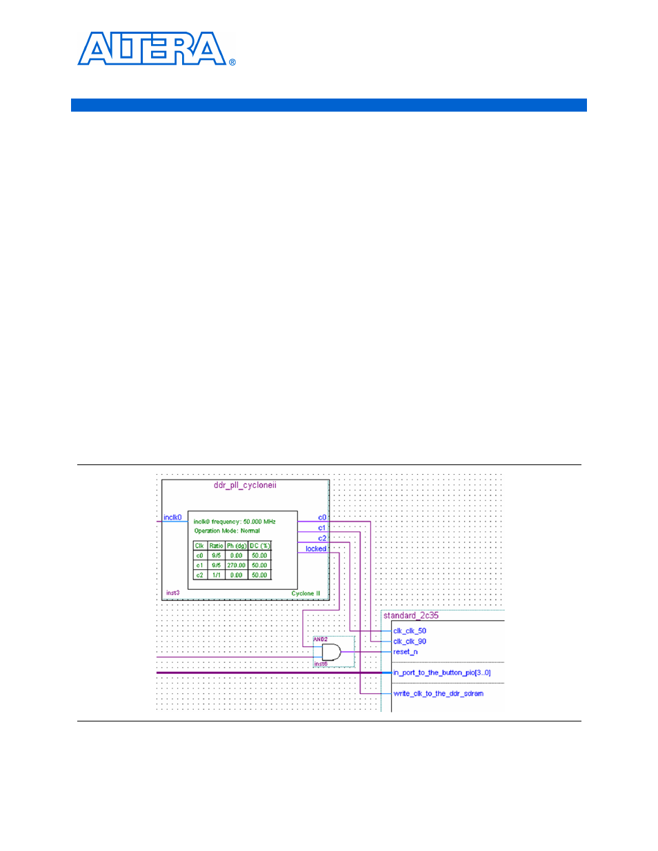
2. During the generation of an SOPC Builder system that contains a DDR SDRAM
controller component, SOPC Builder creates a PLL source file (.v or .vhd) and a
symbol file (.bsf) to synthesize the DDR SDRAM clocks. The PLL source and
symbol file names are ddr_pll_cycloneii. This PLL must be instantiated at the top
level of the design and should drive the DDR write_clk signal and the main
system clock. The c1 output of the PLL has a 270º phase shift and is the PLL
output that you should connect to the DDR SDRAM controller’s write_clk.
1
Use the same PLL to drive both the DDR SDRAM write clock and the system clock, to
reduce clock skew between the two clocks.
shows an example of how you
should connect the PLL in a top-level schematic for an SOPC Builder system that
contains a DDR SDRAM controller and two system clocks.
Figure B–1. Example of DDR SDRAM PLL Connections