Efer to, Ddr sdram initialization timing, Nop (for 200 ms, programmable) – Altera DDR SDRAM Controller User Manual
Page 61: Extended lmr (elmr), Nop (for 200 clock cycles, fixed)
Chapter 3: Functional Description
3–25
Interfaces & Signals
© March 2009
Altera Corporation
DDR and DDR2 SDRAM Controller Compiler User Guide
DDR SDRAM Initialization Timing
f
DDR SDRAM and DDR2 SDRAM initialization timing is different. For DDR2 SDRAM
initialization timing, refer to
“DDR2 SDRAM Initialization Timing” on page 3–26
The DDR SDRAM controller initializes the SDRAM devices by issuing the following
memory command sequence:
■
NOP (for 200 ms, programmable)
■
PCH
■
Extended LMR (ELMR)
■
LMR
■
NOP (for 200 clock cycles, fixed)
■
PCH
■
ARF
■
ARF
■
LMR
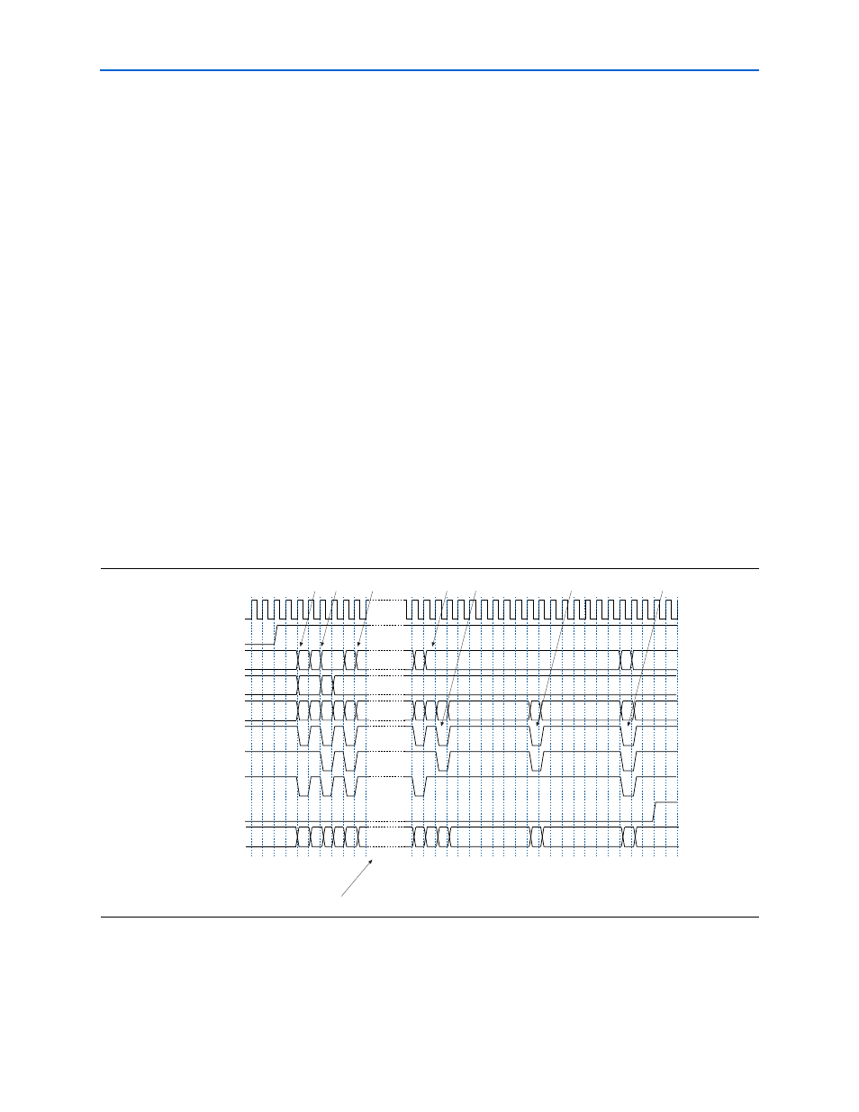
shows a typical initialization timing sequence, which is
described below. The length of time between the reset and the first PCH command
should be 200 ms. This time can be reduced for simulation testing by setting the start-
up timer parameter in IP Toolbench.
1. A PCH command is sent to all banks by setting the precharge pin, the address bit
a[10]
, or a[8] high.
Figure 3–17. DDR SDRAM Device Initialization Timing
clk
ddr_cke
ddr_a
ddr_ba
ddr_cs_n
ddr_ras_n
ddr_cas_n
ddr_we_n
local_init_done
0
0
0
1
0
1
0
0
0
0
0
0
0
0
[1]
[2]
[3]
[4]
[6]
[5]
[5]
200 clock cycles
Key:
P = PCH
L = LMR
A = ARF
DDR Command
P
L
L
P
A
A
L
L