Altera DDR SDRAM Controller User Manual
Page 63
Chapter 3: Functional Description
3–27
Interfaces & Signals
© March 2009
Altera Corporation
DDR and DDR2 SDRAM Controller Compiler User Guide
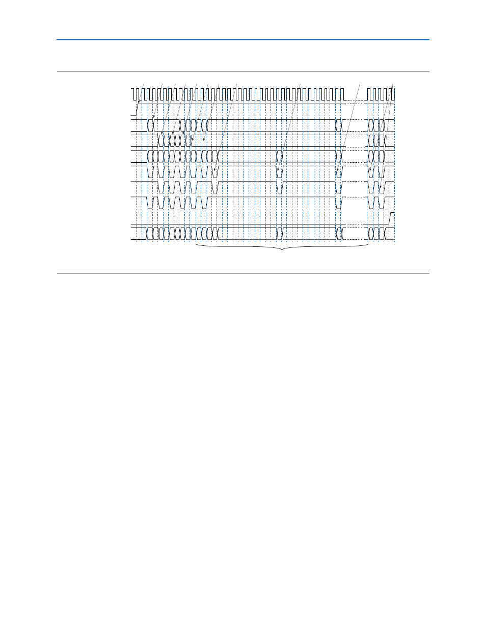
1. The clock enable signal (CKE) is asserted 200
μs after coming out of reset.
2. The controller then waits 400 ns and then issues the first PCH command by setting
the precharge pin, the address bit a[10] or a[8] high. The 400 ns is calculated by
taking the number of clock cycles calculated by the wizard for the 200
μs delay and
dividing this by 500. If a small initialization time is selected for simulation
purposes, this delay is always at least 1 clock cycle.
3. Two ELMR commands are issued to load extend mode registers 2 and 3 with
zeros.
4. An ELMR command is issued to extend mode register 1 to enable the internal DLL
in the memory devices.
5. An LMR command is issued to set the operating parameters of the memory such
as CAS latency and burst length. This LMR command is also used to reset the
internal memory device DLL.
6. A further PCH command places all the banks in their idle state.
7. Two ARF commands must follow the PCH command.
8. A final LMR command is issued to program the operating parameters without
resetting the DLL.
9. 200 clock cycles after step
, two ELMR commands are issued to set the memory
device off-chip driver (OCD) impedance to the default setting.
The DDR2 SDRAM controller asserts the local_init_done signal, which shows
that it has initialized the memory devices.
Figure 3–18. DDR2 SDRAM Device Initialization Timing
Key:
P = PCH
L = LMR
A = ARF
clk
ddr_cke
ddr_a
ddr_ba
ddr_cs_n
ddr_ras_n
ddr_cas_n
ddr_we_n
local_init_done
DDR Command
2 0 3 0 1 0
0
1 0 1 1
1
0
0
0
0
0
0
0
P
L
L
L
L
P
A
A
L
N
L
L
L
200 clock cycles
[1]
[2]
[3]
[3]
[4]
[7]
[6]
[5]
[7]
[8]
[9]