Altera DDR SDRAM Controller User Manual
Page 53
Chapter 3: Functional Description
3–17
Device-Level Description
© March 2009
Altera Corporation
DDR and DDR2 SDRAM Controller Compiler User Guide
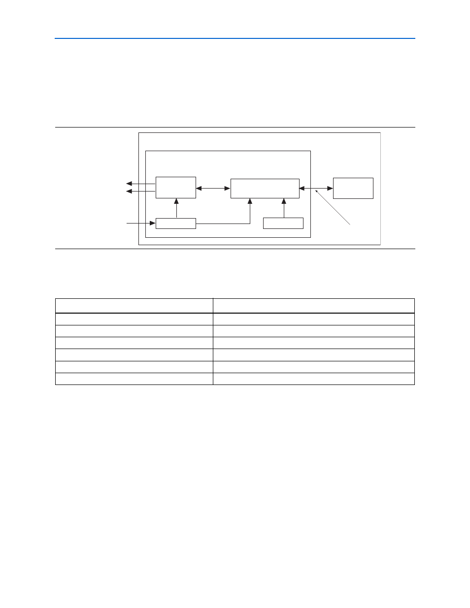
shows the testbench and the example design.
1
Ensure that the example driver is not optimized away in your example design, by
preserving the pnf output. Either attach it to a pin or assign it as a virtual pin in your
Quartus II project.
describes the files that are associated with the example design and the
testbench.
The example driver is a self-checking test generator for the DDR or DDR2 SDRAM
controller. It uses a state machine to write data patterns to a range of column
addresses, within a range of row addresses in all memory banks. It then reads back
the data from the same locations, and checks that the data matches. The pass not fail
(pnf) output transitions low if any read data fails the comparison. There is also a
pnf_per_byte
output, which shows the comparison on a per byte basis. The
test_complete
output transitions high for a clock cycle at the end of the write or
read sequence. After this transition the test restarts from the beginning.
The data patterns used are generated using an 8-bit LFSR per byte, with each LFSR
having a different initialization seed.
Figure 3–12. Testbench & Example Design
Example Dri
v
er
PLL
clock_source
test_complete
pnf
Example Design
Testbench
DDR SDRAM Controller
DDR SDRAM
DIMM Model
Bidrectional Board
Delay Model
DLL
Table 3–5. Example Design & Testbench Files
Filename
Description
Testbench for the example design.
Example design.
ddr_pll_
Example PLL.
ddr_fb_pll_stratixii.v or .vhd
Optional fed-back PLL (Stratix II devices only).
Example driver.
Top-level description of the custom MegaCore function.
Notes to
(1)
(2) Replace