Intermediate resynchronization registers, Dqs postamble, Dqs postamble” on – Altera DDR SDRAM Controller User Manual
Page 88: Intermediate, Ming
A–10
DQS Postamble
DDR and DDR2 SDRAM Controller Compiler User Guide
© March 2009
Altera Corporation
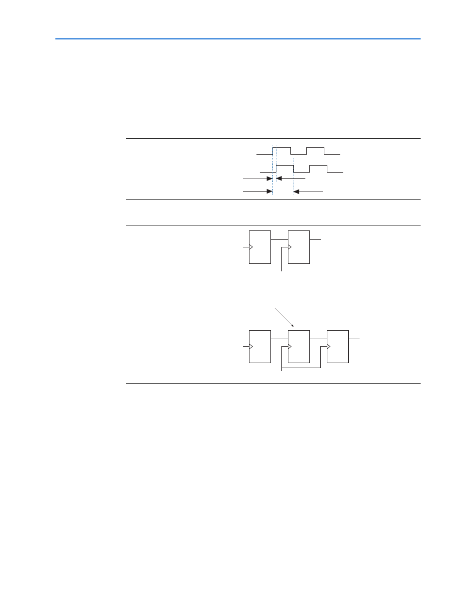
Intermediate Resynchronization Registers
shows the time available to latch the data from the resynchronization
registers, T1. This time T1 may not be sufficient to latch the data properly. If the
negative edge of the system clock latches data, there is time T2 to latch the
resynchronized data. To latch the data with the negative system clock edge, turn on
Insert an intermediate resynchronization register
(refer to
).
DQS Postamble
The DDR and DDR2 SDRAM DQ and DQS pins use the SSTL I/O standard. When
neither the FPGA nor the SDRAM device are driving the DQ and DQS pins, the
signals go to a high-impedance state. Because a pull-up resistor terminates both DQ
and DQS to V
TT
the effective voltage on the high-impedance line is V
TT
. According to
the specification for the SSTL I/O standard, this state is an intermediate logic level
and the input buffer may interpret it as either a logic high or logic low. If there is any
noise on the DQS line, the input buffer may interpret the noise as strobe edges.
When the DQS signal transitions to a high-impedance state after a read postamble,
you must disable the DQS capture registers. This action ensures the captured data is
not corrupted before it is successfully resynchronized.
Figure A–6. Time Between Resynchronization and System Clock
Figure A–7. Inserting an Intermediate Resynchronization Register
System Clock
T1
Resynchronization
Clock
T2
System Clock
Intermediate
Register
Resynchronization
Clock
System Clock
Resynchronization
Clock