Figure a–2 on, Fer to, Figure a–2 – Altera DDR SDRAM Controller User Manual
Page 84

A–6
Resynchronization
DDR and DDR2 SDRAM Controller Compiler User Guide
© March 2009
Altera Corporation
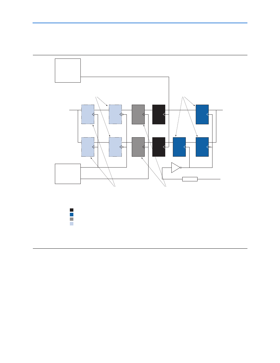
shows the resynchronization registers for Stratix II devices with DQS
capture and optional fed-back clock (refer to
Figure A–2. Resynchronization Registers—Stratix II Devices with Fed-back Resynchronization
Notes to
(1) IP Toolbench automatically inserts the intermediate resynchronization registers, depending on your choice of resynchronization phase.
(2) IP Toolbench automatically inserts these registers if the design needs them.
clk
PLL
DQS
Clocked by delayed DQS Clock
DQ
local_rdata
resynch_clk
Reclock resynchronized data
to rising edge registers
(see Note 2)
Fed-back PLL
(Optional)
fedback_
resynch_clk
90
o
Intermediate resynchronization registers
(see Note 1)
Resynchronization registers
Capture registers
Clocked by Fed-back Clock
Clocked by Resynchronization Clock
Clocked by System Clock
