Controller timings, Controller timings –37, Figure 3–22 – Altera DDR SDRAM Controller User Manual
Page 73: Figure 3–21
Chapter 3: Functional Description
3–37
Parameters
© March 2009
Altera Corporation
DDR and DDR2 SDRAM Controller Compiler User Guide
shows the DLL reference clock options.
Controller Timings
The memory timing parameters on the controller timings tab adjust the controller’s
timing to meet the timing parameters specified in the datasheet for the memory
devices. The Controller Timings tab shows the following three columns of
information:
■
Required
■
Cycles
■
Actual
The Required column specifies the timing requirements from the memory device
datasheet; these requirements can be minimum or maximum times. The values in the
required column are automatically set by your chosen memory device from the
Memory Device
list.
The Cycles column specifies the number of cycles that the controller uses to meet
these timing requirements.
The Actual column reports the actual time that the controller uses, based on the
values in the cycles column and the clock speed.
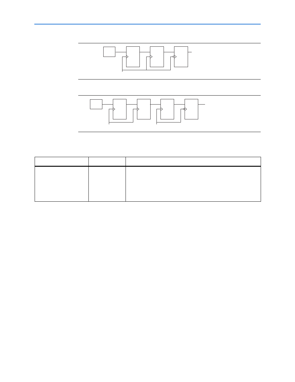
Figure 3–21. Additional Pipeline Registers—A = On, B = Off, C= On
Figure 3–22. Additional Pipeline Registers—A = On, B = On, C= On
Negative Edge
Address and Command
Output
B
clk
FSM
A
Negative Edge
Address and Command
Output
addrcmd_clk
clk
FSM
A
B
Table 3–17. DLL Reference Clock Options
Parameter
Range
Description
Insert logic to allow the DLL
to update only during the
memory refresh period
On or off
For Stratix devices, Altera recommends you turn on this option to switch
off the DLL during read operations and so reduce jitter. For Stratix II
devices, Altera recommends you turn on this option only if your memory
interface spans two sides of the device or if you intend to share a DLL
between two or more interfaces on two sides of the device. Refer to
.