Altera DDR SDRAM Controller User Manual
Page 47
Chapter 3: Functional Description
3–11
Device-Level Description
© March 2009
Altera Corporation
DDR and DDR2 SDRAM Controller Compiler User Guide
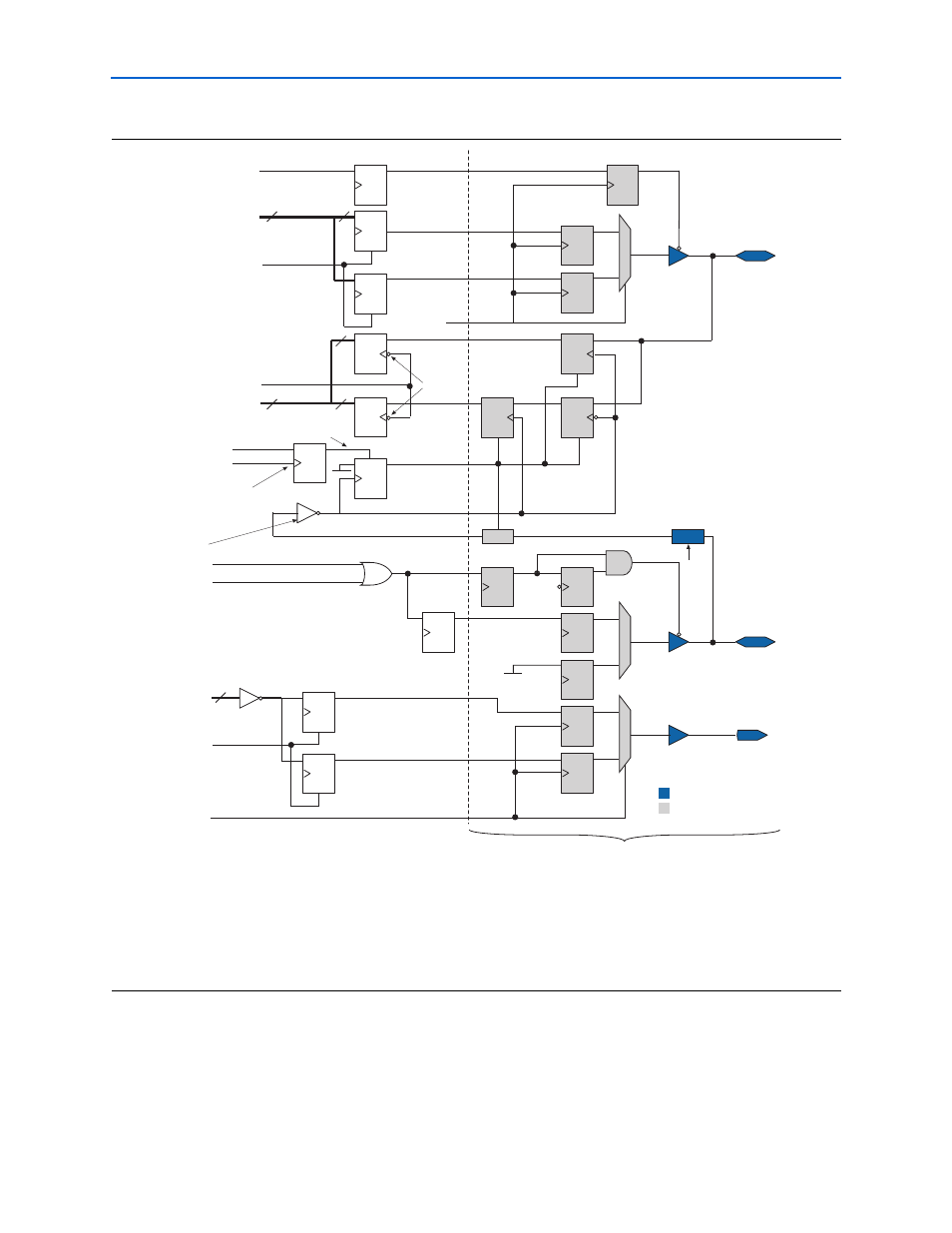
Figure 3–6. Cyclone II DQS Group Block Diagram
Notes to
(1) This figure shows the logic for one dq output only. A complete byte group consists of eight times the DQ logic with the DQS and DM logic.
(2) All clocks are clk, unless marked otherwise.
(3) Each DQS requires a global clock resource. Invert combout of the ALTDDIO_BIDIR megafunction for the DQS pin before feeding in to inclock
of the ALTDDIO_BIDIR megafunction for the DQ pin.
(4) The optional inverters are controlled by the resynchronization edge and postamble edge settings on the Manual Timing tab, refer to
D Q
D
write_clk
altddio Megafunctions
dqs
dm
(Note 3)
dqs_oe
1
Delay
Ao
Bo
DQS_A
OE
B
OE
Clock Delay
Control Circuit
Clock Control Block
Q
0
1
D Q
D Q
0
1
D Q
D Q
Q
Q
D
D
be
doing_wr
dqs_burst
Q
D
2
Q
D
Q
D
Q D
Q D
Q D
Q D
Q D
D
Q
Q
Q
D Q
D
D
Q
D Q
wdata
dq
write_clk
doing_wr
rdata
dq_enable_reset
postamble_clk
resynched_data
dq_enable
dq_capture_clk
resynch_clk
dq_oe
16
DQ_A
OE
Ao
C
A
B
Bo
0
1
16
8
8
8
D
EN
EN
doing_wr
EN
EN
wdata_valid
Preset (asynchronous)
I
I
I
IOEs
FPGA LEs
Optional Inverter (Note 4)
Optional Inverters (Note 4)
EN
EN