Signals, Signals –28 – Altera DDR SDRAM Controller User Manual
Page 64
3–28
Chapter 3: Functional Description
Interfaces & Signals
DDR and DDR2 SDRAM Controller Compiler User Guide
© March 2009
Altera Corporation
Signals
shows the DDR and DDR2 SDRAM controller system signals.
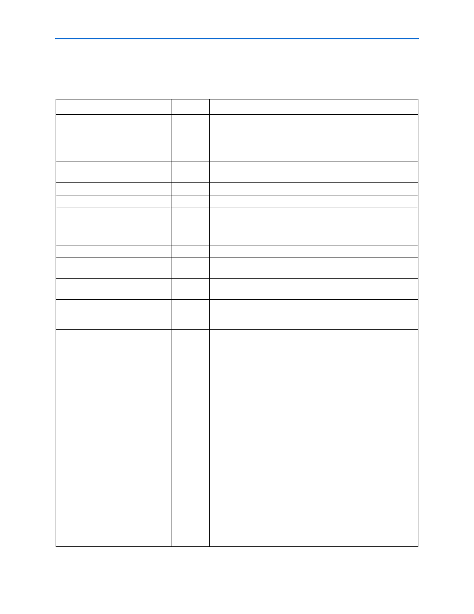
Table 3–7. System Signals (Part 1 of 2)
Signal Name
Direction
Description
addrcmd_clk
Input
The clock to the address and command output registers. Only
available if Insert extra pipeline registers in the datapath is on. The
addrcmd_clk
signal allows you to adjust the address and
command output timing, if required. The addrcmd_clk signal is
connected to the system clock by default.
capture_clk
Input
Optional clock that can be used instead of DQS to capture read data,
for example in the Stratix side banks.
clk
Input
System clock.
dqs_delay_ctrl[5:0]
Input
Control bus from the DLL to the DQS pins.
dqsupdate
The Stratix II DLL generates the dqsupdate signal for the DQS pins to
control when the DQS delay chain value can update. Only available if
the interface is on a single side of the device and Insert logic to allow
the DLL to update during the memory refresh period is off.
fedback_clock_in
Input
Fed-back clock input.
postamble_clk
Input
The postamble logic clock, which disables the capture registers before
the end of the DQS read postamble period.
reset_n
Input
System reset, which can be asserted asynchronously but must be
deasserted synchronous to the rising edge of the system clock.
Input
Clock that resynchronizes read data from the DQS clock domain to the
system clock domain. Typically, you can use the system clock as the
resynchronization clock.
resynch_clk_edge_select
Input
Allows you to switch on a second pair of registers, clocked on the
negative edge of the resynchronization clock, immediately after the
resynchronization registers. This feature allows safer transfer of your
resynchronized read data back to the system clock domain, if your
resynchronization clock phase is variable. It is only available in
designs targetting a HardCopy II device or if a HardCopy II device is
specified as a companion device in your project. By default, the
example design connects the signal to logic zero, which disables the
extra set of registers.
The resynch_clk_edge_select is added to HardCopy II
designs to allow you to safely adjust the resynchronization clock while
still maintaining a safe transfer back to the system clock domain. An
extra set of resynchronization registers are inserted on the opposite
edge and a multiplexer to select which register's output to pass on to
the system clock register (refer to
The output of the capture register goes to the resynchronization
register, which may be clocked on the rising edge of a dedicated PLL
output. The extra logic (a falling edge register and a multiplexer) gets
inserted before the system clock register.
You should keep this select signal programmable if your
resynchronization clock phase can be tuned by the PLL
reconfiguration block. If you tie it off to a fixed value, you may limit the
range across which you can adjust your resynchronization clock.