Memory timings, Memory timings –38 – Altera DDR SDRAM Controller User Manual
Page 74
3–38
Chapter 3: Functional Description
Parameters
DDR and DDR2 SDRAM Controller Compiler User Guide
© March 2009
Altera Corporation
For minimum timing requirements, the values in the actual column must be greater
than or equal to the requirement; for maximum timing requirements, the figure in the
actual column must be less than or equal to the requirement. You can choose whether
to set the values in the cycle column or allow the wizard to choose the most
appropriate values.
shows the memory timing parameters.
Memory Timings
shows memory device datasheet settings. IP Toolbench uses these values
to perform timing analysis.
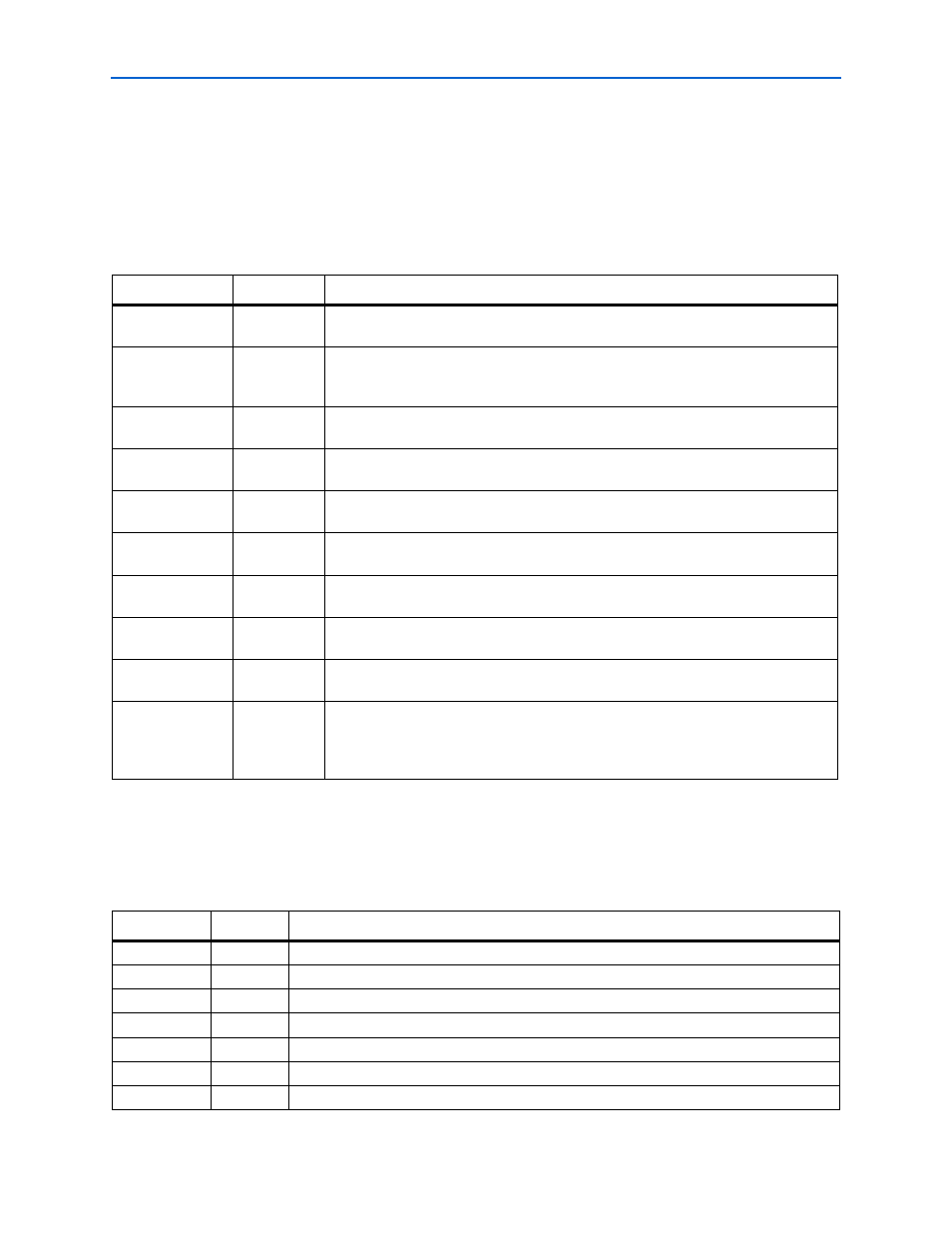
Table 3–18. Memory Timing Parameters
Parameter
Range
Description
Manually choose
clock cycles
On or Off
Turn on, to enter values in the cycles column; turn off and the wizard calculates the
values in the cycles column.
t
REFI
≤ 65534
Interval between refresh commands (maximum). The controller performs regular
refresh at this interval unless user controlled refresh is turned on (refer to
).
t
INIT
≤ 65534
Memory initialization time (minimum). After reset, the controller does not issue any
commands to the memory during this period.
t
RP
2 to 5
Precharge command period (minimum). The controller does not access the memory
for this period after issuing a precharge command.
t
RCD
2 to 5
Active to read-write time (minimum). The controller does not issue read or write
commands to a bank during this time after issuing an active command.
t
RFC
7 to 31
Auto-refresh command period (minimum). The length of time the controller waits
before doing anything else after issuing an auto-refresh command.
t
WR
2 to 5
Write recovery time (minimum). The controller waits for this time after the end of a
write transaction before issuing a precharge command.
t
RAS
4 to 15
Active to precharge time (minimum). The controller waits for this time after issuing an
active command before issuing a precharge command to the same bank.
t
MRD
2 to 3
Load mode register command period (minimum). The controller waits for this time
after issuing a load mode register command before issuing any other commands.
t
WTR
1 to 3
Write to read command delay (minimum). The controller waits for this time after the
end of a write command before issuing a subsequent read command to the same
bank. This timing parameter is specified in clock cycles and so has no entry in the
Required column.
Table 3–19. Device Datasheet Settings (Part 1 of 2)
Parameter
Units
Description
t
DQSQ
ps
The maximum DQS to DQ skew; DQS to last DQ valid, per group, per access.
t
QHS
ps
The maximum data hold skew factor.
t
DQSCK
ps
The access window of DQS from CK/CK#.
t
AC
ps
The access window of DQ from CK/CK#.
t
CK_MAX
ps
The maximum permitted clock cycle time.
t
DS
ps
The minimum DQ and DM input setup time relative to DQS.
t
DH
ps
The minimum DQ and DM input hold time relative to DQS.