Postamble logic – Altera DDR SDRAM Controller User Manual
Page 89

A–11
DQS Postamble
© March 2009
Altera Corporation
DDR and DDR2 SDRAM Controller Compiler User Guide
The DDR and DDR2 SDRAM Controller Compiler provides this DQS postamble logic.
IP Toolbench automatically chooses the best postamble logic clocking scheme for your
system based on the parameters that you enter. The postamble clock can be the
positive or negative edge of either the system clock or the write clock. If a safe
postamble cannot be guaranteed using one of these four phases, a separate output of
the PLL is used as the postamble clock. If the postamble clock phase is close (<90
° ) to
the positive edge of the system clock, an alternative postamble control
synchronization scheme is used.
Postamble Logic
through
show the postamble logic. For Stratix
devices, the dq_enable register clocked by the DQS signal is placed in an LE close to
the associated DQ group to drive their input clock enables. The data input to the
dq_enable
register is set to GND, and the preset is connected to logic generated by
the controller. The postamble logic ensures that the register is released from preset
prior to the last active negative edge of DQS, so that the dq_enable signal goes low
with the last active negative edge of DQS. The input clock enable is therefore disabled
before DQS transitions to high-impedance at the end of the DQS read postamble.
You can specify your own postamble clock instead of using the automatically selected
one, on the Manual Timing tab of the wizard. Also, you can disable the DQS
postamble logic completely, on the Manual Timing tab of the wizard.
DQS postamble logic is not required for DDR and DDR2 SDRAM if you are using a
dedicated read data capture clock (non-DQS mode). As such, in non-DQS mode the
wizard disables the DQS postamble logic.
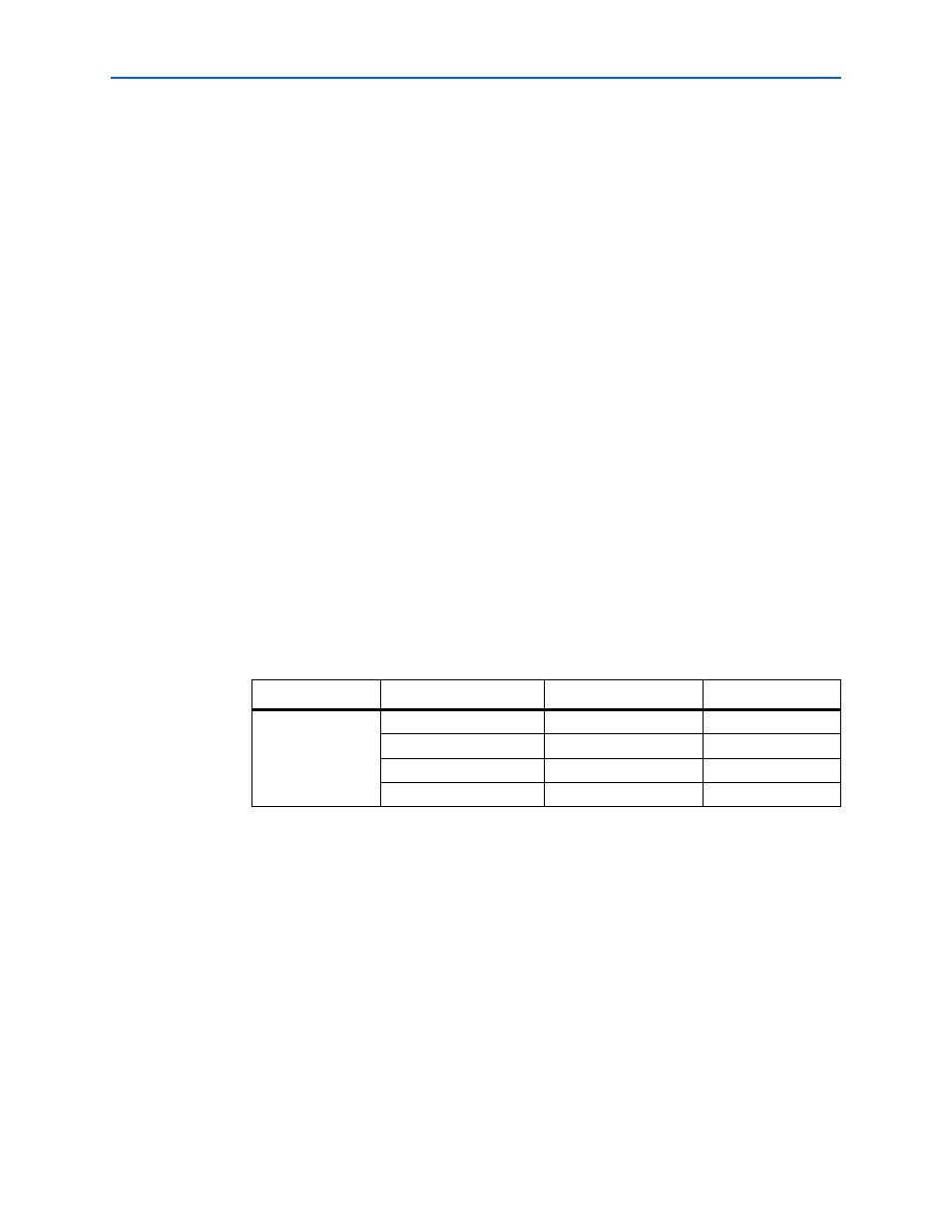
shows the manual postamble parameters.
Table A–6. Manual Postamble Parameters
Cycle
Clock
Edge
Phase (
° )
0, 1, 2, 3, 4, 5, 6
clk
Rising
write_clk
Falling
90
clk
Falling
180
write_clk
Rising
270
Notes to
(1) Postamble cycle 0 phase 0 is defined as the first rising edge of clk capable of generating the postamble enable
preset signal for CAS latency = 2.
(2) Use the intermediate postamble option to guarantee timing
