Writes, Figure 3–13. writes – Altera DDR SDRAM Controller User Manual
Page 56
3–20
Chapter 3: Functional Description
Interfaces & Signals
DDR and DDR2 SDRAM Controller Compiler User Guide
© March 2009
Altera Corporation
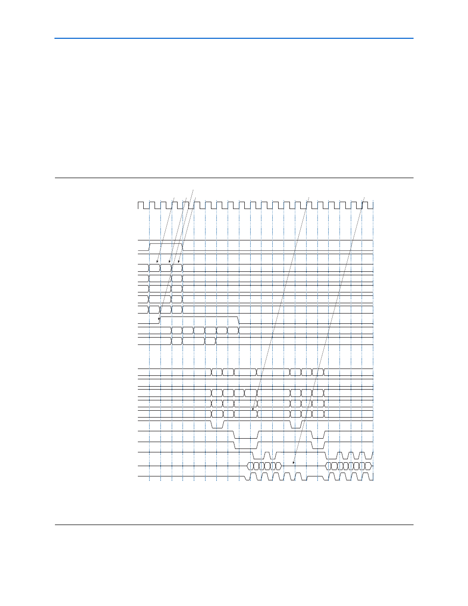
Writes
shows three write requests of different sizes, the first two to
sequential addresses and the third to a new row and bank. The controller allows you
to use any burst length up to the maximum burst length set on the memory device.
For example, if you select burst length of 8 for your DDR SDRAM memory, the
controller allows bursts of length 1, 2, 3, and 4 (2, 4, 6, and 8 on the DDR SDRAM
side).
1
The concept is similar for DDR2 SDRAM although only burst lengths 1 and 2 (2 and 4
on the DDR2 SDRAM side) are available.
Figure 3–13. Writes
Notes to
:
(1) The local_cs_addr, local_row_addr, local_bank_addr, and local_col_addr signals are a representation of the
local_addr
signal.
(2) DDR Command shows the command that the command signals (ddr_ras_n, ddr_cas_n and ddr_we_n) are issuing.
clk
local_read_req
local_write_req
local_ready
local_size
local_cs_addr
(
1
)
local_row_addr
(
1
)
local_bank_addr
(
1
)
local_col_addr
(
1
)
local_wdata_req
local_wdata
local_be
ddr_cs_n
ddr_cke
ddr_a
ddr_ba
DDR Command (
2)
ddr_ras_n
ddr_cas_n
ddr_we_n
ddr_dm(0)
ddr_dq
ddr_dqs(0)
1
2
4
4
1
3
0
3
010
210
000
210
1
3
0
3
020 021 030
000
030
9275FF45 1A27 C510A84BD259
A04A
D259
2
1
3
2
3
F
D
F
D
F
7
F
7
F
7
F
000
010 000 040 042
0000
210 000 060
000
060
0
1
0
1
0
3
0
3
0
3
NOP
ACT NOP
WR
NOP
ACT NOP WR
NOP
WR
DDR SDRAM
Interface
Local Interface
[1]
[3]
[2]
[5]
[4]
[6]