Altera DDR SDRAM Controller User Manual
Page 45
Chapter 3: Functional Description
3–9
Device-Level Description
© March 2009
Altera Corporation
DDR and DDR2 SDRAM Controller Compiler User Guide
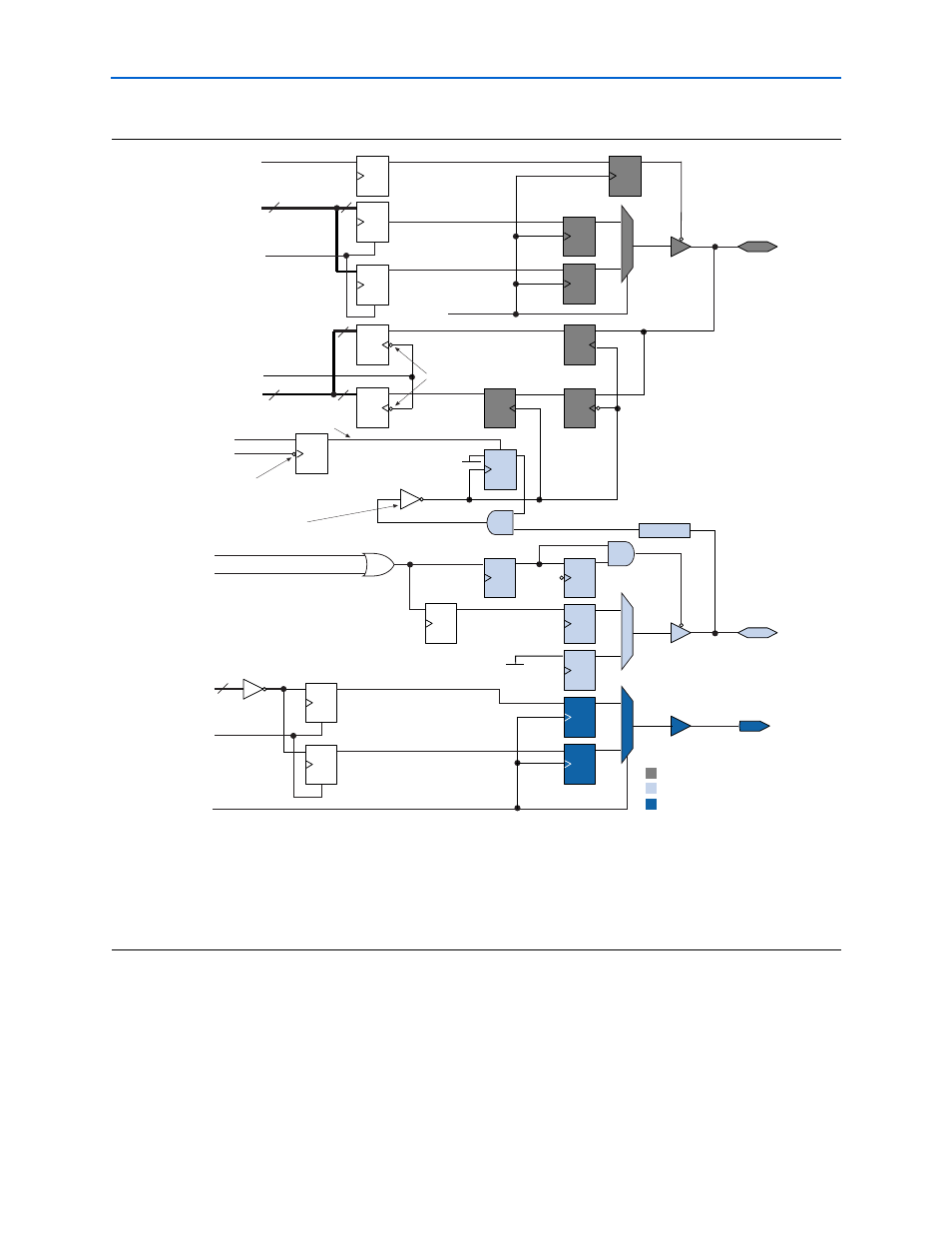
Figure 3–4. Stratix II DQS Group Block Diagram
Notes to
(1) This figure shows the logic for one DQ output only. A complete byte group consists of eight times the DQ logic with the DQS and DM logic.
(2) All clocks are clk, unless marked otherwise.
(3) Invert combout of the I/O element (IOE) for the dqs pin before feeding in to inclock of the IOE for the DQ pin. This inversion is automatic if
you use an ALTDQ megafunction for the DQ pins.
(4) The optional inverters are controlled by the resynchronization edge and postamble edge settings on the Manual Timings tab, refer to
D
Q
D
w
rite_clk
DQS
DM
d
q
s_oe
1
DQS Delay
Ao
Bo
Q
0
1
D
Q
D
Q
0
1
DQS IOEs
DM altddio Megaf
u
nction
D
Q
D
Q
Q
Q
D
D
b
e
doing_
w
r
d
q
s_
bu
rst
Q
D
2
Q
D
Q
D
Q
D
Q
D
Q
D
Q
D
Q
D
D
Q
Q
Q
D
Q
D
D
Q
D
Q
w
data
DQ
w
rite_clk
doing_
w
r
rdata
doing_rd
(pipelined)
postam
b
le_clk
resynched_data
d
q
_capt
u
re_clk
resynch_clk
d
q
_oe
16
0
1
16
8
8
8
D
EN
EN
doing_
w
r
EN
EN
w
data_valid
DQ IOEs
d
q
_ena
b
le_reset
Preset (asynchronous)
(Note 3)
Optional Inverter (Note 4)
Optional Inverters (Note 4)