Datapath, Datapath –2 – Altera DDR SDRAM Controller User Manual
Page 38
3–2
Chapter 3: Functional Description
Block Description
DDR and DDR2 SDRAM Controller Compiler User Guide
© March 2009
Altera Corporation
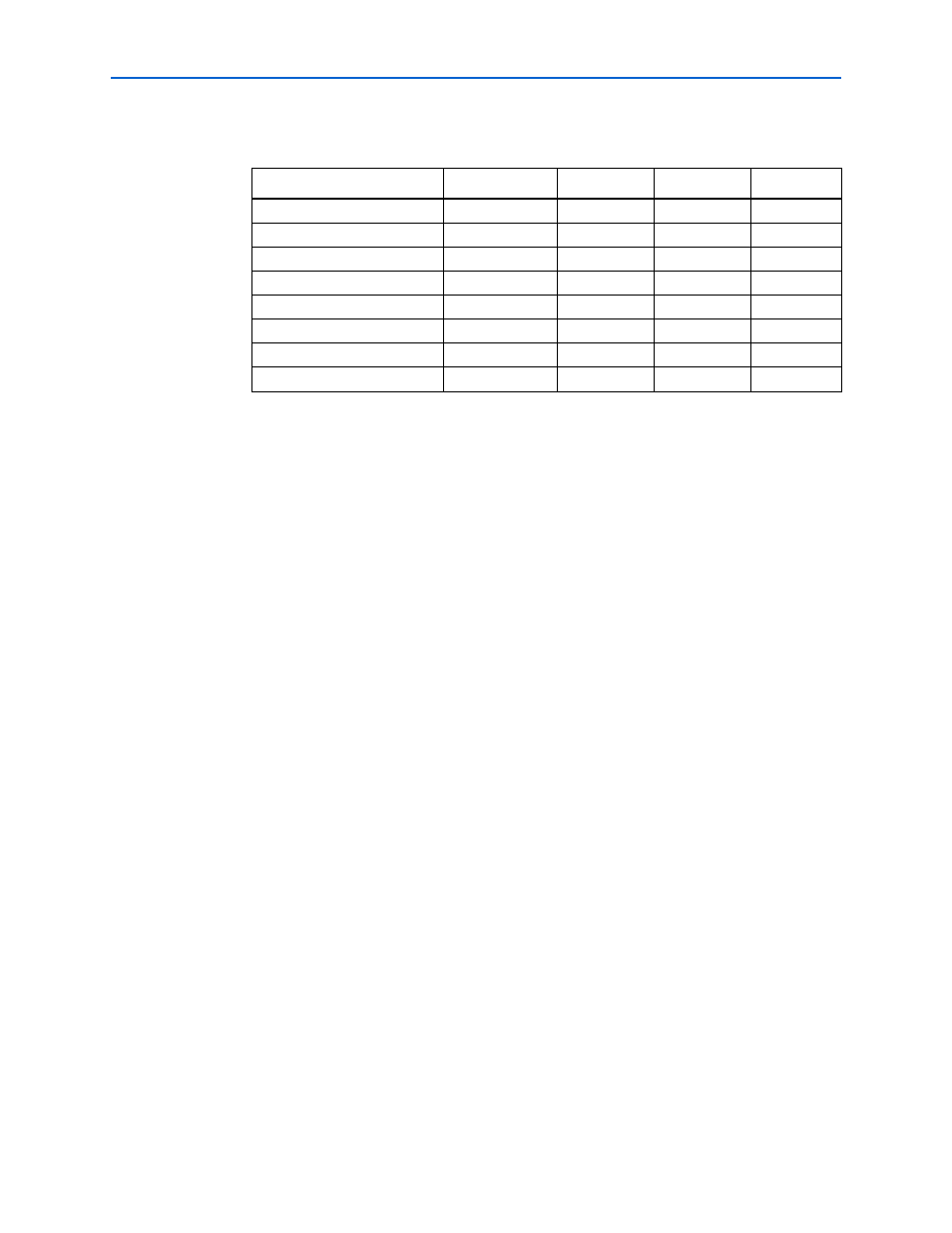
shows the standard SDRAM bus commands.
The DDR and DDR2 SDRAM controllers must open SDRAM banks before they access
addresses in that bank. The row and bank to be opened are registered at the same time
as the active (ACT) command. The DDR and DDR2 SDRAM controllers close the bank
and open it again if they need to access a different row. The precharge (PCH)
command closes a bank.
The primary commands used to access SDRAM are read (RD) and write (WR). When
the WR command is issued, the initial column address and data word is registered.
When a RD command is issued, the initial address is registered. The initial data
appears on the data bus 2 to 3 clock cycles later (3 to 5 for DDR2 SDRAM). This delay
is the column address strobe (CAS) latency and is due to the time required to read the
internal DRAM core and register the data on the bus. The CAS latency depends on the
speed of the SDRAM and the frequency of the memory clock. In general, the faster the
clock, the more cycles of CAS latency are required. After the initial RD or WR
command, sequential reads and writes continue until the burst length is reached or a
burst terminate (BT) command is issued. DDR and DDR2 SDRAM devices support
burst lengths of 2, 4, or 8 data cycles. The auto-refresh command (ARF) is issued
periodically to ensure data retention. This function is performed by the DDR or DDR2
SDRAM controller.
The load mode register command (LMR) configures the SDRAM mode register. This
register stores the CAS latency, burst length, and burst type.
f
For more information, refer to the specification of the SDRAM that you are using.
Datapath
The datapath provides the interface between the read and write data busses of the
local interface and the double-clocked, bidirectional data bus of the memory. The
local data busses are twice the width of the memory data bus width, because the DDR
or DDR2 SDRAM data interface transfers data on both the rising and falling edges of
the clock.
Table 3–1. Bus Commands
Command
Acronym
ras_n
cas_n
we_n
No operation
NOP
High
High
High
Active
ACT
Low
High
High
Read
RD
High
Low
High
Write
WR
High
Low
Low
Burst terminate
BT
High
High
Low
Precharge
PCH
Low
High
Low
Auto refresh
ARF
Low
Low
High
Load mode register
LMR
Low
Low
Low