Altera DDR SDRAM Controller User Manual
Page 42
3–6
Chapter 3: Functional Description
Device-Level Description
DDR and DDR2 SDRAM Controller Compiler User Guide
© March 2009
Altera Corporation
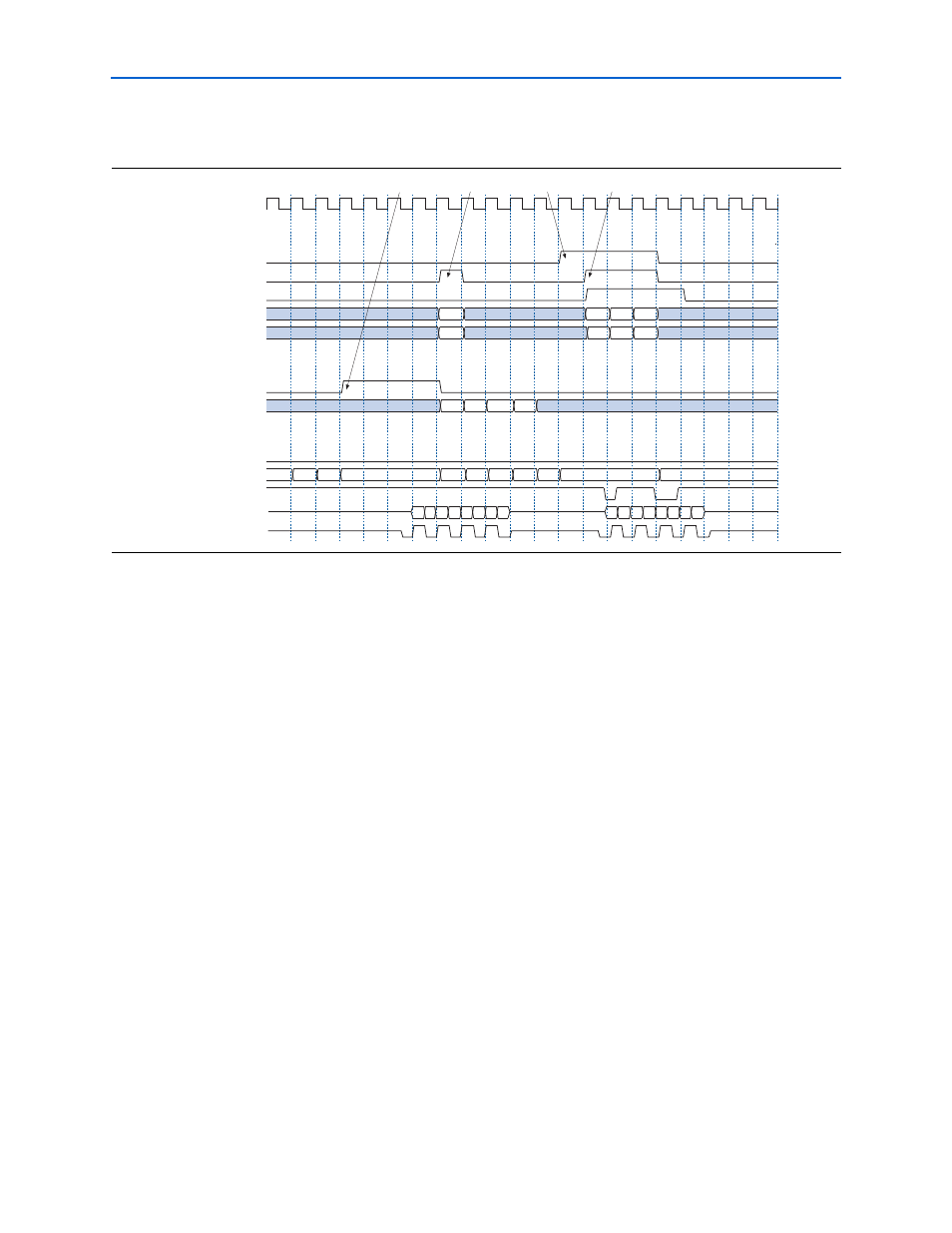
shows the datapath timing (CAS latency is 2.0).
1. The controller asserts control_doing_rd to enable the DQ input registers so
that the read data is captured (the datapath delays this signal to match the CAS
latency). In this case, it is expecting four cycles of read data, so it holds the signal
asserted for four clock cycles. At the end of the burst, the signal is deasserted to
disable the DQ capture registers, which avoids them being clocked unnecessarily
after the DQS read postamble.
2. The controller state machine asserts the control_wdata_valid signal as soon
as it knows that it is doing a write. The signal does not need to be asserted this
early. However, in this example it simplifies the controller design. The write data
is only valid in that clock cycle and is held in the wdata registers until the write
happens.
3. The controller asserts control_doing_wr for the length of the burst (four beats)
to indicate that it is doing a write. This signal controls the output enables of the
DQ signals.
4. The controller reasserts control_wdata_valid to request the next write data
once it knows it is now writing to the memory
1
If you use DDR2 SDRAM and design your own controller, you need to take
the variable write latency into account when generating the
control_doing_wr
signal.
Figure 3–3. Datapath Timing
clk
Write Interface
control_doing_wr
control_wdata_valid
control_wdata
control_be
Read Interface
control_doing_rd
control_rdata
DDR SDRAM
Interface
DDR Command
ddr_dm
ddr_dq
ddr_dqs
control_dqs_burst
A269
32A0 4671 31F5
31F5
1
0
3
0
0
AD75 D739
D31D3A50
3A50
NOP ACT NOP
RD
NOP PCH NOP ACT NOP
WR
NOP
WR
[1]
[3]
[2]
[4]