Memory, Memory –32, Fer to – Altera DDR SDRAM Controller User Manual
Page 68: Memory” on
3–32
Chapter 3: Functional Description
Parameters
DDR and DDR2 SDRAM Controller Compiler User Guide
© March 2009
Altera Corporation
Memory
shows the memory interface parameters.
shows the memory property parameters.
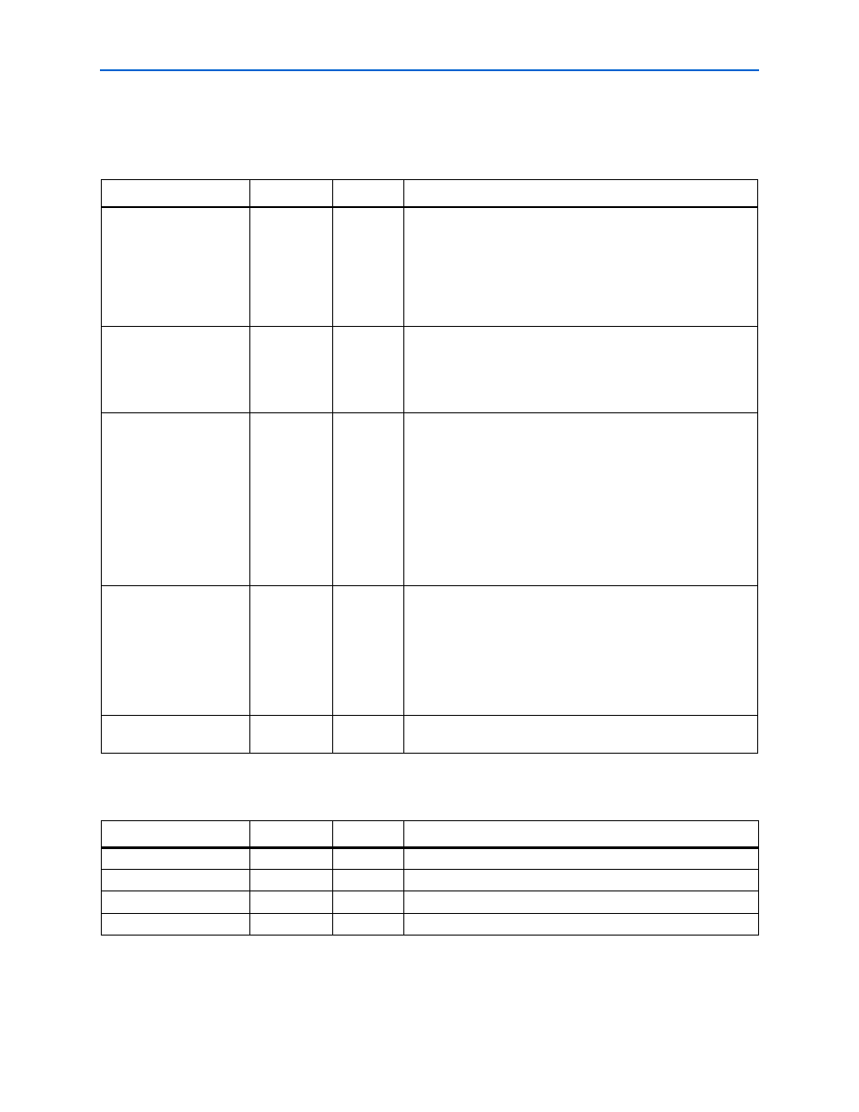
Table 3–11. Memory Interface Parameters
Parameter
Value
Units
Description
Data bus width
≥ 8
Bits
The width of your DDR or DDR2 SDRAM data interface. Your local
interface is twice the width of the memory interface. This value
depends on:
■
The memory
■
Bandwidth requirement
■
Number of DDIO pins available on the selected FPGA device
Number of chip selects
1, 2, 4, or 8
—
The number of chip selects in your memory interface. This is
equivalent to the depth of your memory in terms of number of
chips. This value depends on the type of memory DIMM selected.
If there are two DIMMs and the memory modules on both DIMMs
have two ranks, the number of chip selects is 4.
Number of chip selects
per DIMM
1 or 2
—
The number of chip selects on each DIMM in your memory
system. This option is completely dependent on the type of
external SDRAM that you are using. SDRAMs may come in two
memory chips (called rank) connected in parallel, with only a
unique chip enable signal. This configuration allows the two ranks
to share address and data lines. Selectively asserting only one
chip enable signal at a time, allows twice the memory depth
compared with only a single chip.
If there are two memory chips in the memory module, select 2,
otherwise select 1.
Use dedicated PLL
outputs
On or off
—
Turn on to use dedicated PLL outputs to generate the clocks,
which is recommended for HardCopy II devices.
HardCopy II designs use dedicated PLL outputs for noise
immunity, better signal integrity, and minimal variation over
process, temperature, and voltage.
When turned off, the ALTDDIO megafunction generates the clock
outputs.
Number of clock pairs
from FPGA to memory
1 to 6
—
The number of differential clock pairs driven from the FPGA to the
memory. More clock pairs reduce the loading of each output.
Table 3–12. Memory Property Parameters (Part 1 of 2)
Parameter
Range
Units
Description
Row address bits
10 to 14
Bits
The number of row address bits for your memory.
Column address bits
8 to 13
Bits
The number of column address bits for your memory.
Bank address bits
2 or 3
Bits
The number of bank address bits for your memory.
Precharge address bit
8 or 10
–
The address bit to use as the precharge pin.