Read-write-read-write, Figure 3–15. read-write-read-write – Altera DDR SDRAM Controller User Manual
Page 59
Chapter 3: Functional Description
3–23
Interfaces & Signals
© March 2009
Altera Corporation
DDR and DDR2 SDRAM Controller Compiler User Guide
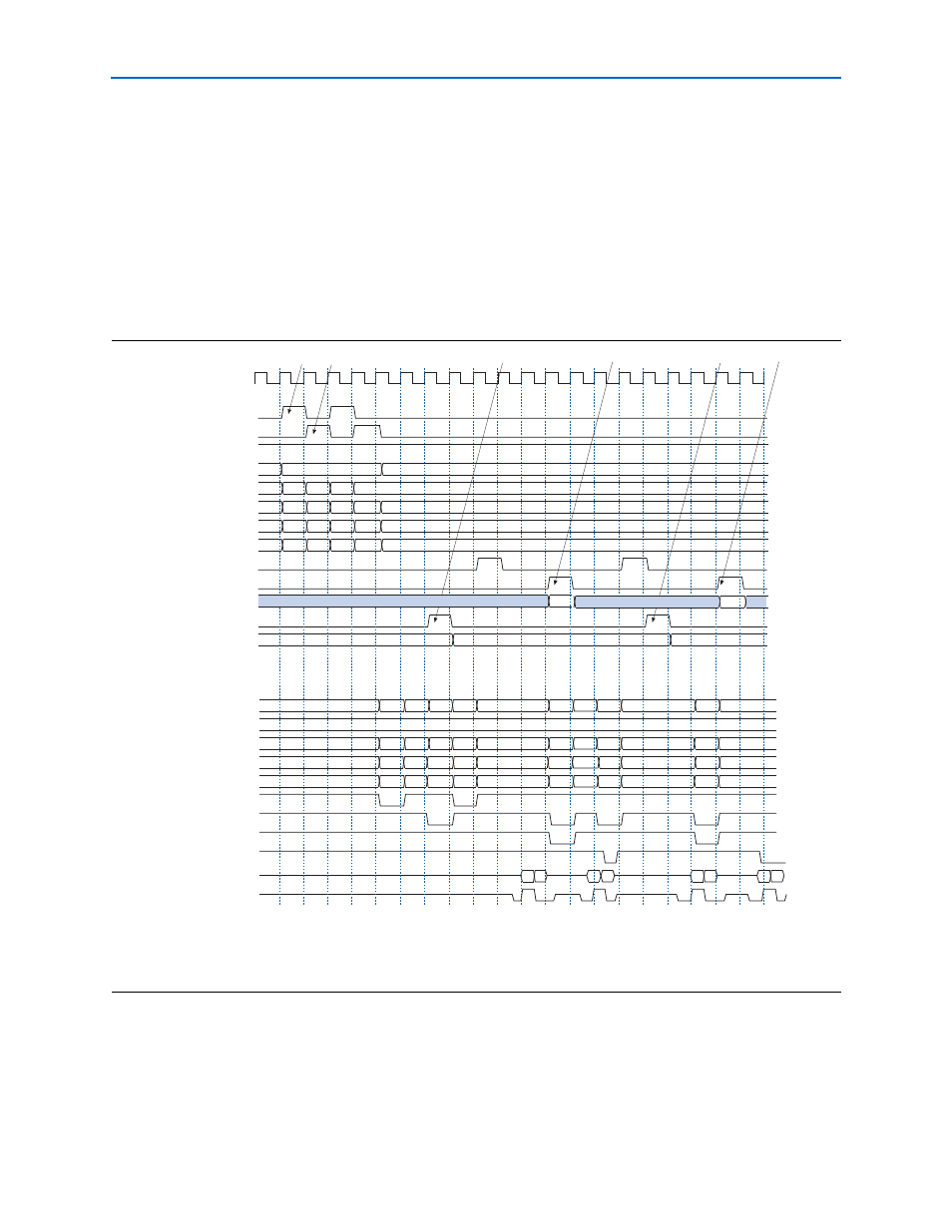
4. The controller returns the read data for the first request by asserting the
local_rdata_valid
signal. The exact number of clock cycles between the
controller accepting the request and returning the data depends on the number of
other requests pending in the controller, the state the memory is in, and the timing
requirements of the memory (e.g., the CAS latency).
5. The controller returns the read data for the subsequent read requests.
Read-Write-Read-Write
shows a sequence of interleaved reads and writes.
1. The user logic requests a read request by asserting the local_read_req signal
along with the size and address for that read. Because the local_ready signal is
high, that request can be considered accepted.
Figure 3–15. Read-Write-Read-Write
Notes to
:
(1) The local_cs_addr, local_row_addr, local_bank_addr, and local_col_addr signals are a representation of the
local_addr
signal.
(2) DDR Command shows the command that the command signals are issuing.
clk
local_read_req
local_write_req
local_ready
local_size
local_cs_addr (
1
)
local_row_addr (
1
)
local_bank_addr (
1
)
local_col_addr (
1
)
local_rdvalid_in_n
local_rdata_valid
local_rdata
local_wdata_req
local_wdata
ddr_cs_n
ddr_cke
ddr_a
ddr_ba
DDR Command (
2
)
ddr_ras_n
ddr_cas_n
ddr_we_n
ddr_dm
ddr_dq
ddr_dqs
0
0
1
0
2
0
2
0
2
0000 0143 0021 0143
0000
0021
0
1
2
1
0
2
000 019 086 01A
000
085
FFD0
9A38
DF08
D5CD
14D9
D5CD
FF
FB
FF
FB
FE
FF
FE
FF FB
FF
FE
FF
FE
FF
0000
0143 0000 0032 0021
0000
010C0000 0034
0000
010A
0000
010A
0
1
0
1
2
0
2
0
1
0
2
0
2
NOP
ACT NOP RD ACT
NOP
WR NOP RD
NOP
WR
NOP
WR
DDR SDRAM
Interface
Local Interface
[1]
[2]
[3]
[4]
[6]
[5]