Intermediate postamble registers, Intermediate – Altera DDR SDRAM Controller User Manual
Page 90
A–12
DQS Postamble
DDR and DDR2 SDRAM Controller Compiler User Guide
© March 2009
Altera Corporation
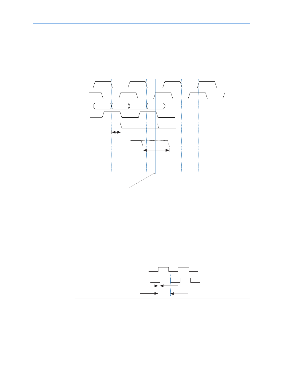
shows an example of how to choose the best postamble phase. In this
example the best postamble phase is cycle = 0, phase = 270
° , and the rising edge of
write_clk
.
This example is for CAS latency = 2. For CAS latency = 2.5, add 180
° to the
calculation; for CAS latency = 3, add 1 cycle.
Intermediate Postamble Registers
shows the postamble clock phase close to the negative edge of the system
clock and the time available for the register to latch the doing_rd_delayed signal is
T1. If the time T1 is not sufficient to latch the data properly, clock the register that
outputs doing_rd_delayed signal with the positive edge of the system clock,
which is time T2 to latch the doing_rd_delayed data and is larger than T1. To latch
the data with the positive edge of the system clock, turn on Insert an intermediate
postamble register
(refer to
).
Figure A–8. Choosing the Best Postamble Phase
clk
H
L
0
0
1
2
180
0
180
write_clk
H
L
Theoretical Postamble
Preset Enable Window
Actual Postamble
Preset Enable Window
dq
dqs (90 shifted)
Postamble
Phase
Postamble
Cycle
o
Theoretical Round Trip Delay
Safe Postamble Window
Best Postamble Phase
Figure A–9. Time Between Postamble and System Clock
System Clock
T1
Postamble
Clock
T2